
Understanding the Arduino Ecosystem: Beyond the Blink Sketch
When makers ask, "How does the Arduino work?", they are usually referring to the seamless abstraction layer that hides complex microcontroller unit (MCU) operations behind simple C++ functions. However, as projects scale from basic LED blinking to high-speed sensor polling and IoT telemetry, understanding the underlying silicon architecture becomes critical. Whether you are working with the legacy 8-bit AVR chips or the modern 32-bit ARM Cortex-M4 boards introduced in recent years, the core principles of memory mapping, peripheral registers, and clock domains remain foundational.
This quick-reference FAQ and architectural guide breaks down the hardware and software pipelines of the Arduino platform, providing the deep technical context required for advanced debugging and circuit design in 2026.
Quick-Reference Hardware Matrix (2026 Lineup)
The Arduino lineup has evolved significantly. While the classic Uno R3 remains a staple in education, the Uno R4 series has become the standard for professional prototyping. Below is a comparison of the core architectures.
| Feature | Uno R3 (Classic) | Uno R4 Minima | Uno R4 WiFi |
|---|---|---|---|
| Core MCU | ATmega328P (8-bit AVR) | Renesas RA4M1 (32-bit ARM) | Renesas RA4M1 + ESP32-S3 |
| Clock Speed | 16 MHz | 48 MHz | 48 MHz (MCU) / 240 MHz (WiFi) |
| Logic Level | 5V DC | 5V Tolerant (3.3V native) | 5V Tolerant (3.3V native) |
| ADC Resolution | 10-bit (0-1023) | 14-bit (0-16383) | 14-bit (0-16383) |
| Avg. Retail Price | $27.00 | $32.00 | $45.00 |
Core Architecture FAQ
1. What exactly happens when I click "Upload" in the IDE?
The upload process is a multi-stage pipeline that bridges your high-level code and the physical silicon. When you click upload, the Arduino IDE invokes a compiler toolchain (like avr-gcc for 8-bit boards or arm-none-eabi-gcc for 32-bit boards). Your .ino files are concatenated, pre-processed, and compiled into machine code, generating a .hex or .bin file.
For classic AVR boards, the IDE uses a utility called avrdude to push this binary over the USB-to-Serial bridge (such as the ATmega16U2 or CH340 chip). The main MCU relies on a tiny piece of pre-flashed memory called the bootloader (typically Optiboot, which occupies just 512 bytes of the 32KB flash). The bootloader listens to the UART RX pin for a specific handshake sequence immediately after a hardware reset. Once verified, it writes the new application code into the remaining flash memory and jumps to the start of your setup() function. Modern ARM-based boards like the Uno R4 utilize bossac or native USB DFU (Device Firmware Upgrade) protocols, bypassing the need for a separate USB-to-Serial bridge chip and allowing for vastly faster upload speeds.
2. How does the Arduino read analog sensors?
Microcontrollers are inherently digital; they only understand binary highs (1) and lows (0). To read a continuous voltage from a sensor (like a potentiometer or an analog temperature sensor), the Arduino uses an Analog-to-Digital Converter (ADC). According to the Microchip ATmega328P datasheet, the classic Arduino uses a 10-bit Successive Approximation Register (SAR) ADC.
When you call analogRead(A0), the MCU configures the ADMUX register to connect the physical pin A0 to the internal sample-and-hold capacitor. The ADC then compares this voltage against a reference voltage (defaulting to the board's VCC, usually 5V or 3.3V). It performs a binary search, taking roughly 13 clock cycles to resolve the voltage into a 10-bit integer (0 to 1023). Therefore, on a 5V Uno R3, each step represents approximately 4.88mV (5V / 1024). The newer Renesas RA4M1 found in the Uno R4 upgrades this to a 14-bit ADC, yielding 16,384 discrete steps and drastically reducing quantization noise for precision instrumentation.
3. How does PWM simulate analog output?
The analogWrite() function does not actually output an analog voltage. Instead, it generates a Pulse Width Modulation (PWM) signal—a digital square wave that toggles between 0V and VCC at a high frequency. By varying the "on" time (duty cycle) relative to the "off" time, the average voltage delivered to a load (like an LED or a DC motor via a transistor) changes.
This is handled entirely by hardware timers, freeing the main CPU to execute other code. On the ATmega328P, Timer0 and Timer2 operate at roughly 490 Hz, while Timer1 (pins 9 and 10) operates at 490 Hz by default but can be reconfigured to 31.25 kHz for audio applications or high-speed motor control to push the switching noise above the human hearing range. The IDE writes your 0-255 duty cycle value directly into the Output Compare Registers (e.g., OCR1A), and the silicon handles the pin toggling automatically.
4. Why do we need a USB-to-Serial bridge chip?
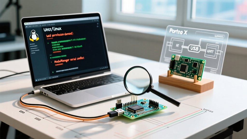
The main MCU (like the ATmega328P) communicates using UART (Universal Asynchronous Receiver-Transmitter) over TX and RX pins, which operate at standard logic levels (0V and 5V). However, modern computers only have USB ports, which use complex differential signaling and packet-based protocols. A secondary chip—historically the ATmega16U2, and commonly the CH340C on budget clones—acts as a translator. It enumerates as a virtual COM port on your PC's operating system and translates USB packets into raw UART serial data, bridging the gap between your PC and the microcontroller's bootloader.
Troubleshooting Quick-Matrix: Hardware Edge Cases
Even with the robust Arduino Documentation and community support, hardware-level failures frequently stall projects. Use this matrix to diagnose low-level silicon and circuit issues.
| Symptom | Root Cause | Hardware / Software Fix |
|---|---|---|
| Random Resets / Brownouts | VCC dropping below 2.7V under load (e.g., when a servo motor engages). | Add a 470µF electrolytic decoupling capacitor across the 5V and GND rails near the motor driver. Power motors from a separate supply. |
| Erratic ADC Readings | High-impedance sensor (>10kΩ) failing to charge the internal S&H capacitor in time. | Add a 100nF ceramic capacitor between the analog pin and GND, or use an op-amp voltage follower as a buffer. |
| USB Enumeration Fails | ESD strike or overcurrent event damaged the USB bridge chip or polyfuse. | Check the 500mA resettable PTC polyfuse near the USB port. If the bridge chip is hot to the touch, replace the board or use an external FTDI programmer. |
| Bootloader Corruption | Uploading via ICSP without restoring the bootloader, or severe memory pointer bugs. | Use a secondary Arduino as an "ArduinoISP" to reburn the bootloader via the ICSP header pins (MISO, MOSI, SCK, Reset). |
Expert Insights: Logic Level Translation
Critical Warning for Mixed-Voltage Systems: As of 2026, the maker ecosystem is heavily split between 5V legacy sensors and 3.3V modern modules (like the ESP32 or nRF52840). Feeding a 5V signal directly into a 3.3V GPIO pin on an Uno R4 or ESP32 will permanently degrade or destroy the silicon's input protection diodes. Always use a bidirectional logic level shifter (such as the TXS0108E or a discrete BSS138 MOSFET circuit) when bridging 5V and 3.3V domains.
Summary
Understanding how the Arduino works requires looking past the simplified IDE functions and examining the microcontroller's registers, clock domains, and physical limitations. By mastering the distinctions between 8-bit AVR and 32-bit ARM architectures, utilizing hardware timers for PWM, and respecting the electrical boundaries of GPIO pins, you transition from a casual hobbyist to an embedded systems engineer capable of designing robust, production-ready hardware.