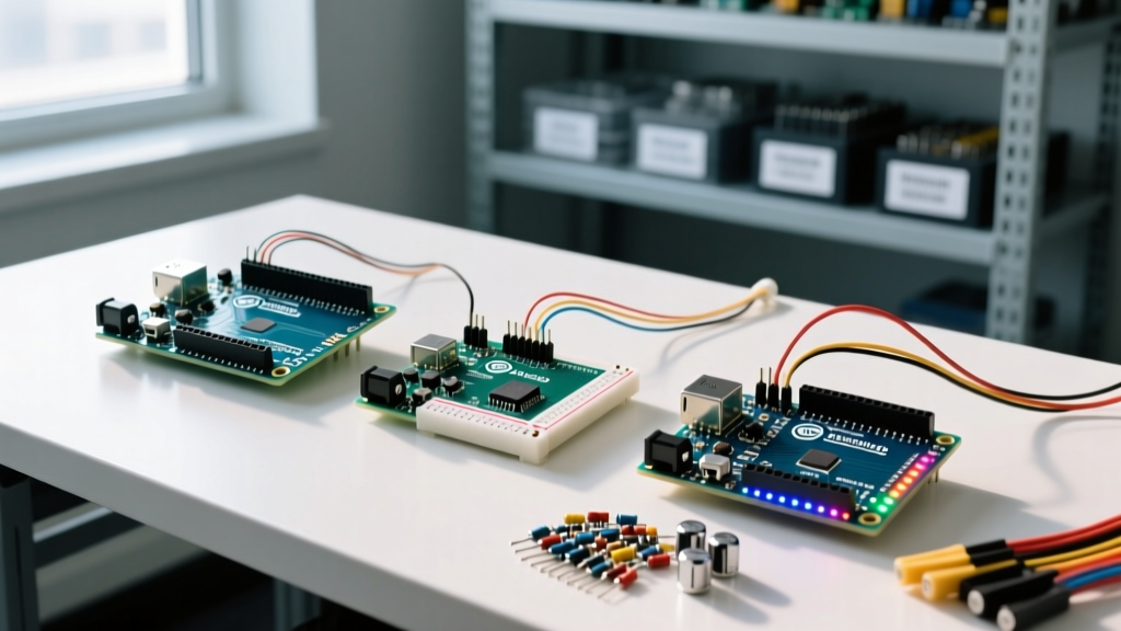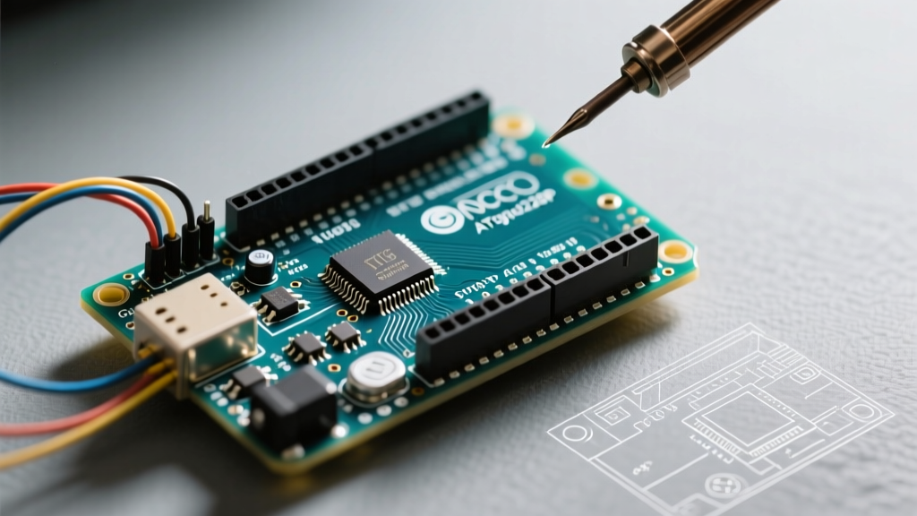

Why the Arduino Uno Schematic Dictates Project Viability
While the Arduino ecosystem has expanded significantly by 2026 with the release of the R4 Minima and WiFi variants, the classic Arduino Uno R3 remains the undisputed baseline for embedded systems education and custom shield design. However, treating the Uno as a 'black box' is a primary cause of hardware failure in intermediate DIY projects. To truly determine if the Uno is suitable for your specific application—whether it is a high-current motor controller, a precision data logger, or a battery-powered IoT node—you must analyze the official Arduino Uno R3 schematic.
Understanding the schematic reveals the hidden bottlenecks: thermal limits of the onboard voltage regulators, the exact routing of the analog-to-digital converter (ADC) references, and the multiplexing constraints of the ATmega328P-PU. This guide breaks down the Uno's hardware architecture to help you make an informed project suitability decision.
Power Architecture: The LDO Thermal Bottleneck
The most misunderstood aspect of the Uno schematic is the power regulation stage. The board utilizes an NCP1117ST50T3G low-dropout (LDO) linear regulator in a SOT-223 package to step down the barrel jack input an external 12V power supply into the LDO, the voltage drop is 7V.
With a maximum power dissipation of roughly 1.5W for the SOT-223 package (assuming adequate PCB copper pour for heatsinking), the maximum continuous current you can safely draw from the 5V rail is:
I_max = 1.5W / 7V = ~214mA
This 214mA must power the ATmega328P (which draws roughly 20mA), the ATmega16U2 USB interface, onboard LEDs, and any external sensors or shields. If your project requires a 5V relay module (drawing ~70mA) and an LCD backlight (~50mA), you are already pushing the thermal limits of the LDO at 12V input.
Critical Design Rule: If your project requires more than 150mA on the 5V rail, do not use the barrel jack. Instead, feed a regulated 5V source directly into the '5V' header pin, completely bypassing the onboard LDO. Be aware that this bypasses the reverse-polarity protection diode (D1) and the auto-reset circuitry.The Auto-Switching Circuit: LMV358 and FDT45P
A brilliant but often overlooked feature in the Uno schematic is the automatic power source selection. When both USB and the barrel jack are connected, the board must prevent 5V from the barrel jack's LDO from backfeeding into the USB VBUS line, which could damage your host computer.
The schematic achieves this using an LMV358 dual operational amplifier configured as a comparator, alongside a FDT45P P-channel MOSFET. The comparator monitors the voltage at the barrel jack through a resistor divider. When the external voltage exceeds roughly 6.6V, the op-amp output goes low, turning on the P-channel MOSFET, which physically disconnects the USB 5V line from the system's 5V net.
Project Suitability Impact: If you are designing a project that requires seamless failover between a USB power bank and a wall adapter, the Uno's hardware handles this automatically. However, the FDT45P has a continuous drain current limit of roughly -1.5A, and the USB line is protected by a 500mA resettable PTC polyfuse (F1). Your USB-powered peripherals cannot exceed 500mA without tripping the polyfuse and causing a system brownout.
I/O Routing and ADC Constraints
According to the Microchip ATmega328P datasheet, the microcontroller features a 10-bit ADC with a multiplexed input stage. The Uno schematic routes analog pins A0 through A5 directly to the MCU, but it also routes them as standard digital I/O (D14-D19).
Crucially, the schematic ties the AREF (Analog Reference) pin to the MCU's AREF pin via a simple low-pass filter, but it does not include an onboard voltage buffer. If your project requires high-precision analog readings (e.g., interfacing with a 12-bit external DAC or a precision load cell amplifier), the standard 5V USB rail is too noisy to serve as an ADC reference. You must supply a clean, external reference voltage to the AREF pin, ensuring it never exceeds VCC (5V) to avoid destroying the internal ADC multiplexer.
Hardware I2C and SPI Routing
- I2C: Routed to A4 (SDA) and A5 (SCL), but also broken out to the dedicated 6-pin ICSP header and the separate SDA/SCL pins near the USB connector. The schematic includes 10k pull-up resistors on the main I2C lines? No, the Uno R3 schematic notably omits onboard I2C pull-up resistors, relying on external shields to provide them. This is a vital consideration if you are wiring raw I2C sensors on a breadboard.
- SPI: Strictly routed to pins 11 (MOSI), 12 (MISO), 13 (SCK), and 10 (SS). The ICSP header mirrors these lines. If your project uses an SPI Ethernet shield (like the W5500) alongside an SD card module, you must manage the Chip Select (CS) lines manually in software, as the schematic hardwires no multiplexing logic.
Project Suitability Matrix: Uno vs. Alternatives
Based on the schematic analysis, how does the Uno R3 (priced at roughly $29.50 for genuine boards or $9.00 for clones in 2026) compare to other platforms for specific project types?
| Project Type | Uno R3 Suitability | Schematic Reason | Better Alternative |
|---|---|---|---|
| High-Power Motor Control | Poor | LDO thermal limits; no isolated motor power planes. | Arduino Mega 2560 or custom PCB |
| Battery-Powered IoT | Very Poor | ATmega16U2 and LDO draw ~15mA idle; no deep sleep routing. | ESP32-C3 or Raspberry Pi Pico |
| Industrial Data Logging | Good | DIP-28 MCU is socketed and easily replaceable in harsh environments. | Arduino Uno R4 Minima |
| Custom HID Keyboard | Excellent | ATmega16U2 can be reflashed with custom USB HID firmware. | Arduino Leonardo / Pro Micro |
Common Schematic-Level Failure Modes
When pushing the Uno beyond its intended educational use case, specific schematic vulnerabilities tend to manifest as hardware failures:
- Back-EMF Destroying the 5V Rail: If you connect an inductive load (like a relay coil or small DC motor) directly to the 5V pin without a flyback diode, the collapsing magnetic field generates a voltage spike. The Uno schematic lacks transient voltage suppression (TVS) diodes on the 5V header. This spike will instantly fry the ATmega328P's internal protection diodes.
- ATmega16U2 USB Disconnects: The USB data lines (D+ and D-) pass through a USBLC6-2SC6 ESD protection chip before reaching the 16U2. While this protects against static, it does not protect against ground loops. If your project connects the Uno to a PC via USB while simultaneously grounding the board to a high-current mains-powered system, ground loop currents will melt the PCB traces connecting the USB port to the 16U2.
- Overvoltage on I/O Pins: The absolute maximum rating for any I/O pin is VCC + 0.5V. If you are powering the Uno via the barrel jack at 9V, but accidentally feed 6V into a digital input pin from an external sensor, the internal clamping diodes will conduct, pulling the 5V rail up and potentially resetting or corrupting the MCU's EEPROM.
Final Verdict: When to Choose the Uno
The Arduino Uno R3 documentation and schematic reveal a board designed for robustness, modularity, and ease of repair, rather than raw performance or power efficiency. The socketed ATmega328P-PU, the dedicated ATmega16U2 USB controller, and the auto-switching power circuit make it the ultimate prototyping hub.
However, for production deployments, battery-operated sensor nodes, or projects requiring high-speed SPI/ADC multiplexing, the Uno's schematic limitations become restrictive. Use the Uno to validate your logic and shield compatibility, but be prepared to migrate to a bare ATmega328P custom PCB or an ARM-based platform like the R4 Minima once your schematic-level power and I/O requirements are finalized.