
Why the Arduino Uno R3 Schematic Diagram is Your Migration Roadmap
For millions of makers and engineers, the Arduino Uno R3 is the gateway to embedded systems. However, as project complexity scales—requiring higher clock speeds, native Wi-Fi/Bluetooth, or deeper SRAM buffers—migrating to advanced platforms like the ESP32-S3, Raspberry Pi RP2040, or STM32F4 becomes mandatory. Before you abandon your trusty Uno, you must thoroughly understand the hardware you are leaving behind.
Analyzing the Arduino Uno R3 schematic diagram is not just an academic exercise; it is a critical engineering step. By deconstructing the Uno's power regulation, USB-to-serial bridging, and auto-reset circuitry, you can accurately map your existing peripheral requirements to a new microcontroller unit (MCU) without encountering catastrophic hardware faults or logic-level mismatches. According to the official Arduino hardware documentation, the R3 revision introduced specific I2C and reset pin changes that heavily influence custom PCB design and platform migration.
Deconstructing the Core Schematic Blocks
To migrate effectively, we must isolate the Uno R3 into four primary schematic domains and identify the bottlenecks each presents in 2026.
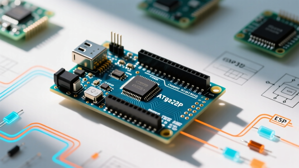
1. The Main MCU: ATmega328P-PU
The heart of the Uno R3 is the Microchip ATmega328P in a DIP-28 package. It operates at 16 MHz with 32 KB of ISP flash memory and a mere 2 KB of SRAM.
- Migration Bottleneck: 2 KB of SRAM is entirely insufficient for modern IoT payloads, TLS encryption handshakes, or audio buffering.
- Modern Alternative: The ESP32-S3 (dual-core 240 MHz, 512 KB SRAM, ~$8.50 for a DevKitC-1 in 2026) or the RP2040 (dual-core 133 MHz, 264 KB SRAM, ~$4.00 for a Pico).
2. USB-to-Serial Bridge: ATmega16U2-MU
Unlike cheaper clones that use the CH340 or CP2102, the official Uno R3 uses a dedicated ATmega16U2 microcontroller programmed as a USB-to-Serial converter.
- Migration Bottleneck: This adds BOM cost, board space, and latency. It lacks native USB OTG (On-The-Go) or high-speed CDC capabilities required for HID keyboards or high-baud-rate data logging.
- Modern Alternative: Platforms with native USB PHYs, such as the STM32F401 or RP2040, eliminate the need for a secondary bridge chip entirely.
Power Delivery Analysis: The LDO Thermal Trap
One of the most common failure modes during platform migration occurs when engineers port a shield or custom circuit to a new board without auditing the power schematic. The Uno R3 utilizes an NCP1117ST50T3G linear drop-out (LDO) regulator to step down the barrel jack input (7V–12V) to 5V.
Engineering Warning: The NCP1117 on the Uno R3 is rated for 1A absolute maximum, but the PCB's thermal pad design limits continuous safe draw to roughly 200mA–300mA at a 12V input before thermal shutdown triggers at 150°C junction temperature.
If your current project draws 500mA from the Uno's 5V pin, you are already pushing the thermal limits of the LDO. When migrating to a custom PCB or a new dev board, you must replace this linear regulation topology with a switching buck converter.
| Uno R3 Schematic Block | Component / Spec | Migration Upgrade (Custom PCB) |
|---|---|---|
| 5V Regulator | NCP1117ST50T3G (Linear, ~300mA safe) | TPS54331 or MP2359 (Buck, 3A+ safe) |
| 3.3V Regulator | LP2985-33 (Linear, 150mA max) | AMS1117-3.3 or dedicated Buck LDO |
| USB 5V Protection | P-MOSFET (NTS2101) & Polyfuse (500mA) | Dedicated USB Load Switch (e.g., TPS2553) |
Signal Integrity and Decoupling Capacitors
A close inspection of the Arduino Uno R3 schematic diagram reveals the decoupling strategy for the ATmega328P. You will find 100nF (0.1µF) ceramic capacitors placed strategically near VCC (Pin 7), AVCC (Pin 20), and AREF.
When migrating to surface-mount equivalents like the ATmega328P-AU (TQFP-32) or transitioning to an STM32, you must replicate and improve this decoupling. Modern high-speed MCUs require a combination of bulk capacitance (10µF–47µF tantalum or low-ESR ceramic) at the power entry point, paired with 100nF capacitors on every single VDD/VDDA pin pair, placed within 2mm of the IC pads. Failing to migrate the decoupling schematic correctly results in erratic ADC readings and spontaneous brownout resets.
The Auto-Reset Circuitry: A Migration Headache
The Uno R3 features a clever auto-reset circuit allowing the IDE to restart the bootloader via the DTR (Data Terminal Ready) signal over USB. The schematic shows a 100nF capacitor in series with the DTR line, connected to the ATmega328P's RESET pin (which is pulled high by a 10kΩ resistor). A 1N4148 diode is placed in parallel to prevent negative voltage spikes.
How This Affects Your Migration
If you are migrating your code and hardware to an ESP32 or a generic STM32 'Blue Pill', this auto-reset schematic is absent.
- ESP32 Migration: The ESP32 uses a different boot-mode selection process requiring GPIO0 to be pulled low during reset. You will need to implement a dual-transistor auto-reset circuit (often using two NPN BJT transistors like the MMBT3904) to replicate the Uno's seamless upload experience.
- STM32 Migration: STM32 chips rely on the BOOT0 pin and NRST. You must manually wire a momentary tactile switch to NRST and configure your IDE to trigger a software reset via SWD (Serial Wire Debug) rather than relying on serial DTR toggling.
GPIO Logic Level Translation Strategy
The Uno R3 operates strictly at 5V logic. Migrating to modern 3.3V platforms requires careful level shifting to prevent frying your new MCU's silicon. According to Texas Instruments' logic translation guidelines, driving a 3.3V CMOS input with a 5V TTL output can cause permanent gate oxide breakdown over time.
Recommended Translation ICs for Migration
- TXS0108E: Excellent for bidirectional I2C and SPI buses (up to 50 Mbps). Requires careful pull-up resistor management.
- SN74LVC8T245: Ideal for unidirectional or parallel data buses, offering high drive strength and independent VCCA/VCCB rails.
- BSS138 MOSFETs: The cheapest, most reliable method for I2C level shifting, replicating the classic Philips application note design.
Step-by-Step Platform Migration Workflow
Use this checklist to transition from the Uno R3 to your target platform:
- Audit the Schematic: Download the Uno R3 PDF and highlight every peripheral connected to your current project. Note whether they rely on 5V tolerances or specific hardware timers (e.g., Timer1 for PWM).
- Calculate True Power Draw: Measure the current on the 5V and 3.3V rails. If 5V draw exceeds 250mA, design a custom carrier board with a switching regulator.
- Map Pinouts via Abstraction: Refactor your Arduino C++ code to remove direct PORTB/PORTD register manipulations. Replace them with
digitalWrite()or hardware abstraction layer (HAL) equivalents to ensure portability. - Design the Interposer: If using a 3.3V dev board, design a simple interposer PCB containing the necessary logic level shifters and 5V buck converter to accept your existing Uno R3 shields.
Final Thoughts on Schematic Literacy
Treating the Arduino Uno R3 as a 'black box' is acceptable for beginners, but fatal for commercial product development. By mastering the Arduino Uno R3 schematic diagram, you transform a simple development board into a comprehensive reference design. You learn exactly why decoupling matters, how USB enumeration is handled, and the physical limits of linear voltage regulation. Armed with this knowledge, your migration to advanced 32-bit ARM or RISC-V platforms will be systematic, electrically sound, and free of the 'magic smoke' failures that plague unprepared engineers.