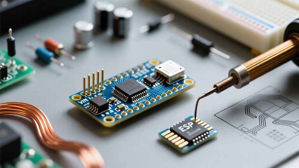

The Anatomy of the Arduino Nano VIN Pin
When transitioning an embedded project from a USB-powered breadboard prototype to a standalone, battery-operated deployment, the Arduino Nano VIN pin becomes the most critical junction on the board. On the classic Arduino Nano (ATmega328P), the VIN (Voltage In) pin is designed to accept an unregulated external power source, nominally between 7V and 12V. This voltage is routed through a reverse polarity protection diode and subsequently into an onboard NCP1117 5.0V linear regulator, which steps the voltage down to the 5V required by the microcontroller and peripheral logic.
However, as the electronics industry shifts toward 3.3V IoT architectures in 2026, engineers migrating legacy Nano designs to modern platforms frequently encounter catastrophic failures. Understanding the exact electrical and thermal limitations of the classic Nano VIN architecture is mandatory before redesigning your power delivery network (PDN) for newer microcontrollers.
Thermal Failure Modes: Why Your Nano Overheats
The most common point of failure when utilizing the Arduino Nano VIN pin is thermal shutdown of the onboard linear regulator. Linear regulators operate by dissipating excess voltage as heat. The power dissipated by the regulator is calculated using the following formula:
P_dissipated = (V_IN - V_OUT) * I_load
Consider a real-world scenario: You are powering a remote environmental sensor node using a 12V sealed lead-acid battery connected to the VIN pin. Your circuit draws 150mA (powering the ATmega328P, an NRF24L01+ radio module, and a BME280 sensor).
- V_IN: 12V
- V_OUT: 5V
- I_load: 0.15A
- P_dissipated: (12 - 5) * 0.15 = 1.05 Watts
The NCP1117 in a standard SOT-223 surface-mount package has a junction-to-ambient thermal resistance (θ_JA) of approximately 50°C/W on a standard 2-layer PCB with minimal copper pours. A 1.05W dissipation results in a temperature rise of 52.5°C above ambient. In a 25°C room, the regulator junction sits at 77.5°C. If this node is deployed in an outdoor enclosure reaching 45°C, the junction temperature spikes to 97.5°C, rapidly approaching the 125°C thermal shutdown threshold and causing erratic brownouts.
Real-World Safe Operating Area (SOA) for Classic Nano VIN
| VIN Input Voltage | Max Continuous Current | Thermal State (SOT-223) | Recommended Use Case |
|---|---|---|---|
| 6.5V - 7.5V | 300 mA | Warm (~45°C rise) | 4x AA NiMH battery packs |
| 8.0V - 9.5V | 150 mA | Hot (~60°C rise) | 9V Alkaline batteries (short duty cycles) |
| 10.0V - 12.5V | 80 mA | Very Hot (~85°C rise) | 12V Lead-Acid / Wall adapters (low power sensors only) |
| > 13.0V | N/A | Thermal Shutdown / Damage | Avoid (Exceeds NCP1117 absolute max ratings) |
Note: Clone boards utilizing unbranded AMS1117-5.0 regulators often exhibit 20% worse thermal performance due to inferior die attach materials and smaller internal copper leadframes.
The Migration Trap: Moving Beyond the Classic Nano
The most dangerous phase of hardware development occurs when migrating a proven classic Nano schematic to a modern 3.3V platform. The pinout may look identical, but the internal power routing of the Arduino Nano VIN architecture changes drastically across modern variants.
Arduino Nano ESP32 (Migration Alert)
Released to meet the demand for native Wi-Fi/BLE in the Nano footprint, the Arduino Nano ESP32 features a completely different power tree. The VIN pin on the Nano ESP32 is not connected to a high-voltage linear regulator. Instead, it is tied directly to the 5V rail (post-USB protection diode).
Critical Warning: If you migrate a legacy design that feeds 12V into the classic Nano VIN pin directly to the Nano ESP32 VIN pin, you will instantly destroy the onboard AP2112K-3.3 LDO and the ESP32-S3 SoC. The Nano ESP32 VIN pin strictly accepts 4.5V to 5.5V.
Raspberry Pi Pico & RP2040 Boards
When migrating to the Raspberry Pi Pico (RP2040), engineers often map the Nano VIN to the Pico’s VSYS pin. The Pico utilizes an RT6150B buck-boost switching regulator. While highly efficient, the VSYS pin has an absolute maximum rating of 5.5V. Feeding 12V into VSYS will cause immediate catastrophic failure of the PMIC. To migrate a 12V design to a Pico, an external DC-DC step-down converter is mandatory.
Platform Migration Power Matrix
Use the following matrix to audit your power delivery network before ordering new PCB revisions or wiring up migration prototypes.
| Platform | VIN / VSYS Pin Function | Acceptable Voltage Range | Onboard Regulator Type | Logic Level |
|---|---|---|---|---|
| Classic Nano (ATmega328P) | High-Voltage Input | 7V - 12V (Recommended) | NCP1117 5.0V (Linear) | 5V |
| Arduino Nano ESP32 | 5V Rail Injection | 4.5V - 5.5V | AP2112K-3.3 (Linear) | 3.3V |
| Arduino Nano 33 IoT | 5V Rail Injection | 4.5V - 5.5V | MIC5366-3.3 (Linear) | 3.3V |
| Raspberry Pi Pico | Main System Input | 1.8V - 5.5V | RT6150B (Buck-Boost) | 3.3V |
| Adafruit QT Py (SAMD21) | 5V Rail Injection | 4.5V - 5.5V | AP2112K-3.3 (Linear) | 3.3V |
Step-by-Step Power Supply Redesign for Migration
To successfully migrate a legacy 12V or 24V industrial design to modern 3.3V platforms without relying on fragile onboard linear regulators, follow this redesign protocol:
- Implement an External Buck Converter: Remove the dependency on the microcontroller board’s VIN pin for high-voltage step-down. Integrate a dedicated switching regulator IC like the Texas Instruments LM2596 or the MPS MP1584EN on your carrier PCB. These modules easily handle 24V inputs and step down to 5V with >85% efficiency, eliminating the thermal bottleneck.
- Route 5V Directly to VUSB / 5V Pins: Once your external buck converter outputs a clean 5V, route this directly to the board’s
5Vpin (bypassing the Nano’s onboard LDO entirely) or theVUSBpin on the Nano ESP32. This eliminates the 0.7V drop from the reverse polarity diode and keeps the board’s thermal footprint near zero. - Add Level Shifting for 5V Peripherals: If your legacy design utilized 5V sensors (e.g., HC-SR04 ultrasonic sensors, 5V I2C LCDs) powered by the Nano’s 5V rail, remember that migrating to the Nano ESP32 or Pico means your GPIO pins are now strictly 3.3V. You must integrate bidirectional logic level shifters (like the NXP PCA9306 or TI TXS0108E) to prevent 5V backfeed from frying the 3.3V SoC.
- Verify USB Backpowering Isolation: When injecting 5V externally, ensure your design includes a Schottky diode (e.g., BAT54S) between the external 5V source and the board’s USB 5V line to prevent current from backfeeding into your PC’s USB port during debugging.
Expert Troubleshooting & Edge Cases
The 'Motor Start' Brownout
Symptom: The Nano resets or behaves erratically the moment a DC motor or relay engages, despite the power supply being rated for high current.
Root Cause: The inrush current of the inductive load causes a momentary voltage sag on the VIN line. If the VIN voltage drops below the NCP1117’s dropout voltage (typically 1.1V to 1.3V), the 5V rail collapses, triggering the ATmega328P’s Brown-out Detection (BOD) circuit.
Fix: Add a low-ESR electrolytic capacitor (470µF to 1000µF) directly across the VIN and GND pins to supply transient inrush current, and ensure the motor is powered from a separate buck converter, not the Nano’s 5V rail.
Clone Board Diode Discrepancies
Official Arduino Nanos utilize a standard silicon rectifier diode for VIN reverse polarity protection, resulting in a ~0.7V drop. Many third-party clones substitute this with a Schottky diode (~0.3V drop) or omit it entirely to save $0.02 per unit. When migrating firmware that relies on precise ADC readings referenced to the 5V rail, this missing voltage drop can introduce a 4% to 8% measurement error if the board is swapped between official and clone variants during manufacturing.
Authoritative References
- Arduino Nano Official Hardware Documentation - Comprehensive schematic and power tree analysis for the classic Nano.
- Onsemi NCP1117 Linear Regulator Datasheet - Thermal resistance metrics and dropout voltage specifications for the SOT-223 package.
- Microchip ATmega328P Datasheet - Brown-out Detection (BOD) thresholds and absolute maximum current ratings for VCC and I/O pins.