
Introduction to Electronic Components Assembly
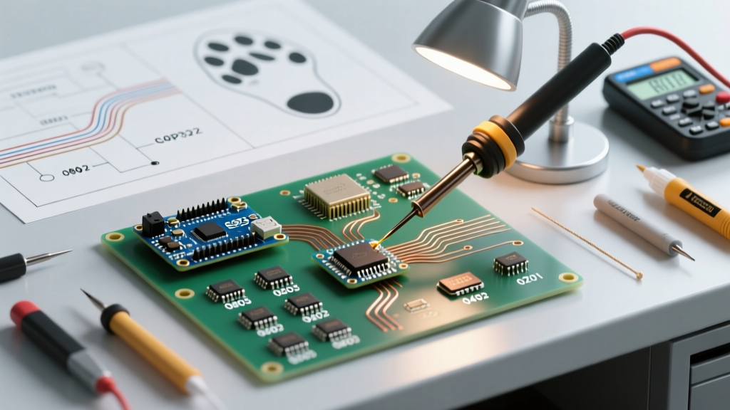
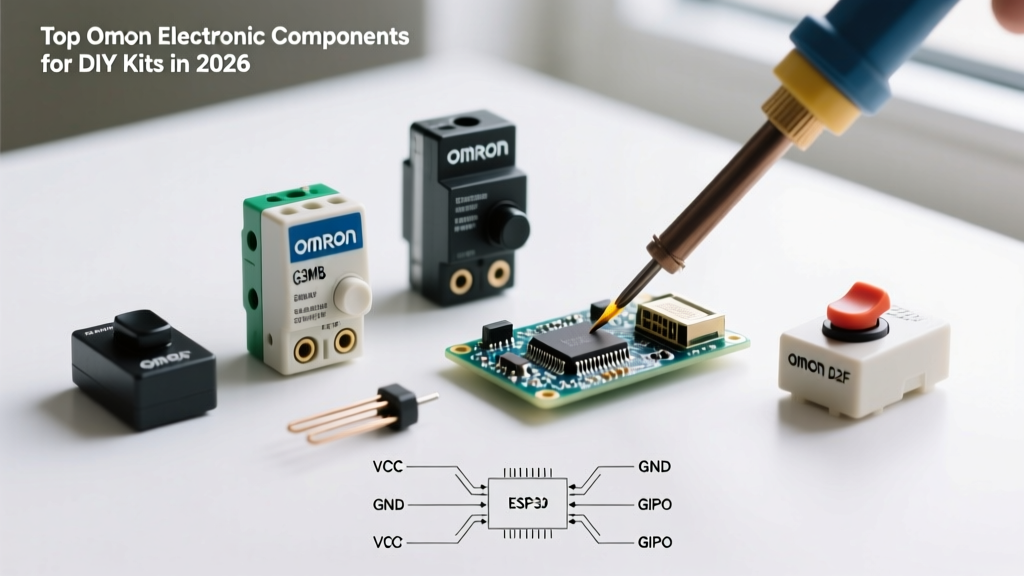
Transitioning from a breadboard prototype to a permanent printed circuit board (PCB) is a major milestone for any DIY electronics enthusiast. The process of electronic components assembly bridges the gap between theoretical schematics and reliable, real-world hardware. While surface-mount technology (SMT) dominates mass manufacturing, through-hole assembly remains the gold standard for beginners, high-voltage applications, and mechanical stress environments.
In this comprehensive tutorial, we will walk through the exact methodologies, tooling, and thermal profiles required for professional-grade through-hole electronic components assembly. Whether you are building a guitar pedal, a custom microcontroller shield, or a linear power supply, mastering these fundamentals will ensure your joints meet industry reliability standards.
Phase 1: Workbench Setup and Tool Selection
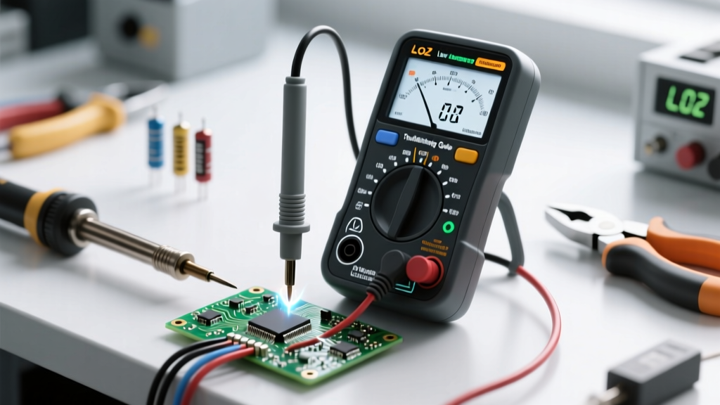
Attempting electronic components assembly with a cheap, unregulated plug-in iron is the fastest way to destroy sensitive silicon and lift copper pads. A proper workbench requires precise thermal control and ergonomic tooling. Below is a curated list of industry-standard tools for beginners and intermediate makers.
| Category | Recommended Model | Est. Price | Why It Matters |
|---|---|---|---|
| Soldering Station | Hakko FX-888D | $105 | Digital temp control, rapid thermal recovery with T18 tips. |
| Solder Wire (Leaded) | Kester 24-6040-00279 (60/40, 0.031") | $35 | Rosin core flux, low melting point (183°C), shiny joints. |
| Flush Cutters | Xuron 170-II Maxi-Shear | $25 | Prevents lead shock and stress fractures on the copper pad. |
| Desoldering Pump | Engineer SS-02 | $25 | Silicone heat shield, tight vacuum seal for clean pad clearing. |
| Tacky Flux | Amtech NC-559-V2-TF | $15 | No-clean formulation, essential for rework and drag soldering. |
Phase 2: Component Sorting and Lead Forming
Before the iron even powers on, proper preparation dictates the success of your electronic components assembly. Components must be sorted by physical height and thermal mass.
The Hierarchy of Placement
Always assemble components from the lowest profile to the highest. This prevents tall components from obstructing your iron's approach angle to lower pads.
- Stage 1: Wire jumpers and bare copper links.
- Stage 2: Resistors, signal diodes (e.g., 1N4148), and small ceramic capacitors.
- Stage 3: IC sockets (Never solder DIP ICs directly; use sockets to prevent thermal death of the silicon).
- Stage 4: Electrolytic capacitors (Verify polarity: the white stripe on the can denotes the negative terminal, matching the shaded side on the PCB silkscreen).
- Stage 5: Connectors, terminal blocks, and tall voltage regulators (e.g., TO-220 packages).
Lead Forming Techniques
Do not bend component leads directly at the component body; this can crack the internal epoxy seal. Use a dedicated lead forming tool or flat-nose pliers (like the Xuron 495) to create a 90-degree bend at least 1.5mm away from the component base. Insert the leads into the PCB and slightly splay them outward (about 5 to 10 degrees) to hold the part flush against the board during soldering.
Phase 3: The 5-Step Soldering Sequence
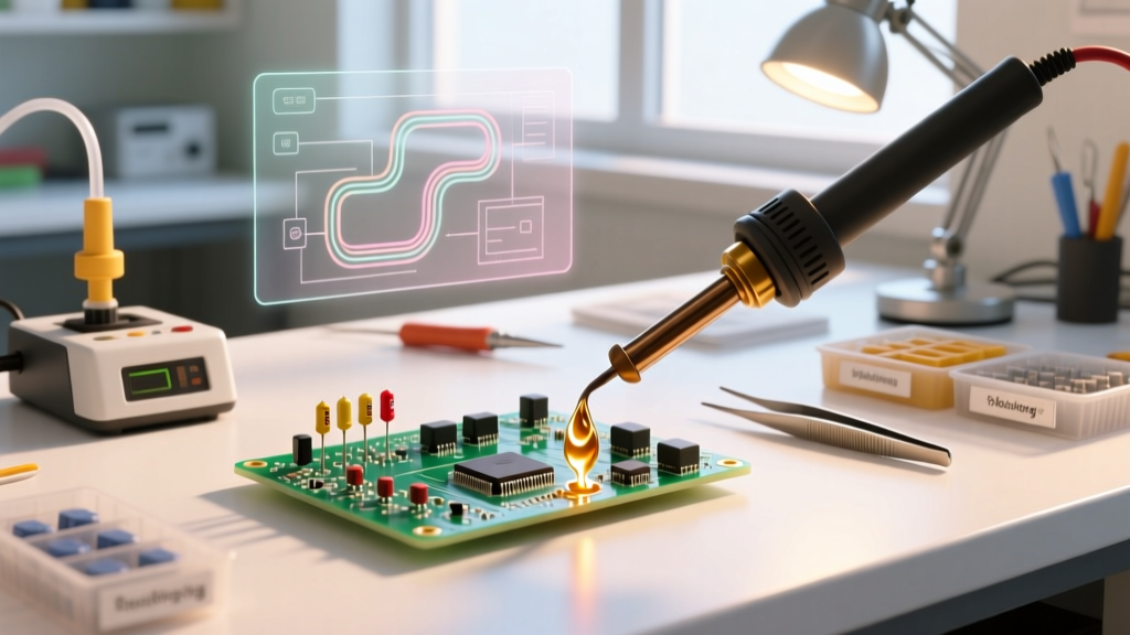
According to SparkFun's Through-Hole Soldering Tutorial, a reliable metallurgical bond requires simultaneous heating of both the pad and the component lead. Set your Hakko FX-888D to 320°C - 340°C for 60/40 leaded solder, or 350°C - 380°C if using SAC305 lead-free alloys.
- Clean and Tin the Tip: Wipe the iron on a damp cellulose sponge or brass wire wool. Apply a tiny amount of fresh solder to the tip to create a thermal bridge.
- Heat the Joint: Place the iron tip so it touches both the copper pad and the component lead simultaneously. Hold for 1 to 1.5 seconds.
- Feed the Solder: Touch the solder wire to the joint, not the iron tip. The flux will activate, bubble, and the solder will flow via capillary action into the plated through-hole.
- Remove Solder, Then Iron: Pull the solder wire away first, then sweep the iron off the pad. Total dwell time should not exceed 3 to 4 seconds to prevent pad delamination.
- Cooling Phase: Hold the board perfectly still. Blowing on the joint or moving the board while the solder is in a plastic state will cause a micro-fracture known as a cold joint.
Pro-Tip: If the solder balls up on the iron tip and refuses to flow onto the pad, you have insufficient flux or oxidation on the pad. Remove the iron, apply a dab of Amtech liquid or tacky flux, and reattempt the joint. As detailed in Adafruit's Guide to Excellent Soldering, flux is the unsung hero of electronic components assembly; it removes oxidation and lowers surface tension.
Phase 4: Inspection and IPC Standards
In professional manufacturing, electronic components assembly is graded against the IPC-A-610 Standard. For most DIY and commercial prototyping, you should aim for Class 2 (Standard Electronic Products) compliance.
Visual Indicators of a Class 2 Joint
- Fillet Shape: The solder should form a smooth, concave fillet that sweeps up the component lead like the inside of a volcano.
- Wetting: The solder must visibly wet both the copper pad and the wire lead, with a contact angle of less than 90 degrees.
- Appearance: Leaded (60/40) solder should be bright and shiny. Lead-free (SAC305) solder will naturally appear dull, matte, and slightly grainy—this is normal and not indicative of a cold joint.
- Fill: For double-sided boards, the solder should ideally wick up through the barrel and be visible on the top layer, though 75% barrel fill is acceptable for Class 2.
Troubleshooting Common Assembly Failures
Even experienced engineers encounter defects. Recognizing and fixing these failure modes is a critical part of mastering electronic components assembly.
1. The Cold Joint
Symptom: The solder looks bulbous, grainy, or dull (on leaded alloys), and fails to wet the pad properly.
Cause: Insufficient heat transfer, moving the component during cooling, or heavy oxidation.
Fix: Apply a small amount of fresh flux to the joint. Reapply the iron for 2 seconds to reflow the solder, then remove and hold still.
2. Solder Bridges (Shorts)
Symptom: A blob of solder connects two adjacent pads or pins, creating an electrical short.
Cause: Using too much solder, using a tip that is too large, or lacking sufficient flux.
Fix: Do not use a solder sucker for bridges. Instead, apply tacky flux and use a 0.050" desoldering braid (like Chemtronics 80-1-5). Press the iron through the braid onto the bridge; capillary action will wick the excess solder away cleanly.
3. Lifted Copper Pads
Symptom: The copper annular ring peels away from the FR4 fiberglass substrate.
Cause: Dwelling the soldering iron on the pad for more than 5-7 seconds, or using excessive mechanical force with a desoldering pump.
Fix: If the pad is completely detached, you must scrape back the solder mask on the connected trace, tin the exposed copper, and solder a small 30 AWG jumper wire to the component lead to restore the circuit.
Safety and Workbench Maintenance
Electronic components assembly involves hazardous materials and high temperatures. Always operate a fume extractor (such as the Hakko FA-400) positioned 6 inches from your work area to capture colophony-based flux smoke, which is a known respiratory sensitizer. If using 60/40 leaded solder, wash your hands thoroughly with soap and water before eating or drinking. Finally, never leave your iron untinned; always apply a thick layer of solder to the tip before powering down the station to prevent the iron plating from oxidizing and pitting in the presence of ambient moisture.