
The Rising Stakes of Component Verification in 2026
As global semiconductor supply chains continue to fragment and re-shore in 2026, the influx of gray-market, counterfeit, and sub-spec electronic components has reached unprecedented levels. According to data tracked by the Electronic Resellers Association International (ERAI), counterfeit incidents involving remarking, die-shrinks, and salvaged parts pulled from e-waste remain a multi-billion dollar liability. For contract manufacturers (CMs), repair depots, and aerospace labs, robust electronic components quality assurance (QA) is no longer optional—it is a critical survival mechanism.
This roundup dissects the essential QA equipment and testing kits required to authenticate, validate, and stress-test electronic components. We bypass generic multimeters and focus on the specialized metrology, non-destructive testing (NDT), and electrical parameter analysis tools that define a modern component verification lab.
Tier 1: Visual and Surface Metrology Kits
The first line of defense against counterfeit components is high-magnification surface inspection. Fraudsters frequently use "blacktopping"—sanding off original manufacturer logos and applying a new epoxy coating to print fake part numbers.
AmScope SM-4TP-BN Trinocular Stereo Microscope
Best for: Mid-volume CMs and advanced repair labs.
Price Range: $450 – $600
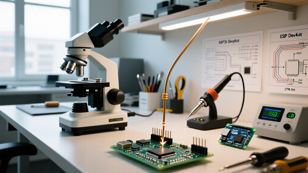
While digital microscopes are popular, a high-quality optical trinocular remains indispensable for detecting surface anomalies. The SM-4TP-BN offers a 7x-45x zoom range. Expert Tip: Always pair this with a 0.5x Barlow lens. This doubles your working distance to roughly 100mm, allowing you to probe IC pins with micro-hooks under the lens without crashing the objective into the component.
Keyence VHX-7000 Digital Microscope System
Best for: High-reliability aerospace and automotive QA labs.
Price Range: $35,000 – $50,000+
For detecting advanced laser-etched counterfeits, optical zoom isn't enough. The VHX-7000 provides 3D surface profilometry. By measuring the exact depth and edge sharpness of the manufacturer's laser etch compared to a Known Good Unit (KGU), QA engineers can spot remarking that is invisible to the naked eye. Original mold marks have distinct depth profiles that aftermarket laser etchers fail to replicate perfectly.
Tier 2: Electrical Parameter and Curve Tracing
Visual inspection cannot detect a "die shrink"—a common counterfeit tactic where a lower-voltage, cheaper silicon die is packaged inside a high-voltage marked casing. Electrical verification is mandatory.
Peak Atlas DCA75 Pro Semiconductor Analyzer
Best for: Quick intake screening and bench-level troubleshooting.
Price Range: $240 – $280
This handheld component analyzer automatically identifies pinouts for BJTs, MOSFETs, and diodes, mapping their junction characteristics. It is an excellent first-pass tool to weed out completely dead or grossly mislabeled discrete semiconductors before they hit the SMT pick-and-place machine.
Keysight B1505A Power Device Analyzer
Best for: Deep I-V curve tracing of power MOSFETs, IGBTs, and SiC/GaN devices.
Price Range: $45,000 – $70,000
As detailed in Keysight's power device analysis documentation, curve tracing is the gold standard for spotting cloned silicon. The B1505A sweeps voltage and current to generate an I-V curve. If a batch of 600V SiC MOSFETs exhibits avalanche breakdown at 420V on the curve tracer, you have definitively proven the batch contains counterfeit, lower-spec dies.
Tier 3: Non-Destructive Internal Inspection (NDT)
When dealing with Ball Grid Arrays (BGAs) and QFNs, the internal architecture is hidden. Non-destructive testing allows labs to inspect die attach, bond wires, and internal delamination without destroying the sample.
FocalSpot Verifier FSX-1000 X-Ray Inspection System
Best for: BGA voiding analysis and bond wire sweep detection.
Price Range: $65,000 – $90,000
Counterfeit or poorly refurbished BGAs often suffer from bond wire sweep or missing wires. The FSX-1000 provides sub-micron voxel resolution, allowing QA techs to count individual 15-micron gold bond wires inside a molded package. Furthermore, it calculates solder void percentages in real-time, ensuring compliance with IPC standards (typically requiring <25% voiding for Class 3 high-reliability assemblies).
Scanning Acoustic Microscopy (SAM) - Sonoscan D9500
Best for: Detecting internal delamination and "popcorning" susceptibility.
Price Range: $120,000+
SAM uses high-frequency ultrasound to detect air gaps inside IC packages. If a component has been improperly stored and absorbed moisture, SAM will reveal delamination between the silicon die and the epoxy encapsulant before the part ever sees a reflow oven.
Equipment Selection Matrix by Lab Volume
Not every facility requires a $100,000 X-ray machine. Below is a decision matrix to help you build an electronic components quality assurance kit that matches your operational scale.
| Lab Scale / Focus | Core Visual Tool | Electrical Testing | NDT / Advanced | Est. Budget |
|---|---|---|---|---|
| Hobbyist / Repair Depot | AmScope Trinocular + Ring Light | Peak Atlas DCA75, Siglent SDS1104X-E | Decapsulation Kit (Chemical) | $1,500 - $3,000 |
| Mid-Volume CM | Dino-Lite Edge Digital Microscope | Keysight 34461A DMM, LCR Meter | Entry-level 2D X-Ray (e.g., Nikon XT V 130) | $25,000 - $45,000 |
| High-Rel / Aerospace | Keyence VHX-7000 Profilometry | Keysight B1505A Curve Tracer | 3D X-Ray, SAM, Thermal Shock Chamber | $200,000+ |
Tier 4: Thermal Profiling and Environmental Stress
A component might pass electrical tests at room temperature but fail catastrophically under load due to poor internal thermal conductivity.
FLIR E54 Advanced Thermal Camera
Best for: Junction-to-case thermal resistance mapping.
Price Range: $4,500 – $5,200
Using the transient dual interface (TDI) method per JEDEC JESD51-14, QA engineers can measure the thermal resistance (RthJC) of power devices. A counterfeit IGBT with a voided die attach will show a thermal delta of 10°C to 15°C higher than a KGU when driven at 50% rated current. The FLIR E54's 320x240 resolution and macro lens accessory make it ideal for spotting these localized hotspots on TO-247 and D2PAK packages.
The 4-Step QA Intake Protocol for Suspect Batches
Equipment is only as good as the methodology driving it. Implement this strict workflow when a batch of components arrives from an unauthorized broker:
- Exterior & Marking Audit: Perform the acetone wipe test. Swab the IC surface with 99% isopropyl alcohol and acetone. If the ink smears, it is a crude remark. Follow up with 40x optical inspection for sanding marks on the edges.
- Dimensional & Coplanarity Check: Use digital calipers and a feeler gauge on a machined granite surface plate. Salvaged parts often have bent leads or warped packages that exceed the 0.08mm coplanarity tolerance required for reliable SMT reflow.
- Decapsulation (Destructive): Select a 5% sample size for chemical decapsulation. Using a fuming nitric acid (98%) drip setup, dissolve the epoxy to expose the silicon die. Read the silicon stepping, mask revision, and manufacturer logo under the microscope. Compare this directly to the manufacturer's datasheet die-revision history.
- Solderability & Bake Test: Perform a solder dip test at 245°C for 3 seconds to verify lead finish wetting. If parts fail, bake them at 125°C for 24 hours to drive out moisture and re-test before rejecting the entire lot.
Expert Insight: Never rely solely on the date code printed on a component. Counterfeiters routinely print recent date codes on salvaged parts from 2015. Always cross-reference the lot traceability codes with the original manufacturer's authorized distribution network, and maintain a physical library of Known Good Units (KGUs) for your most critical BOMs.
Final Thoughts on Building Your QA Arsenal
Investing in electronic components quality assurance equipment is fundamentally about risk mitigation. A single counterfeit $2.00 voltage regulator can cause a $50,000 medical device to fail in the field, leading to catastrophic liability and brand damage. By strategically layering visual metrology, electrical curve tracing, and targeted NDT, your lab can confidently filter out the gray-market noise and ensure that only authentic, spec-compliant silicon reaches your production floor.