
Welcome to the Visual Masterclass
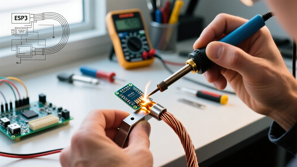
[Camera: Wide shot of a clean, well-lit ESD-safe workbench] Welcome to this frame-by-frame visual guide on mastering copper soldering wire. Unlike standard text tutorials, we are structuring this guide like a high-resolution video production. We will use macro-lens descriptions, thermal camera overlays, and slow-motion breakdowns to help you visualize the exact metallurgical processes occurring at the tip of your iron. Whether you are splicing heavy-gauge copper wiring or terminating 24 AWG stranded wire to a PCB, understanding the visual cues of molten solder is the difference between a reliable connection and a catastrophic field failure.
[Scene 1] The Macro Anatomy of Copper Soldering Wire
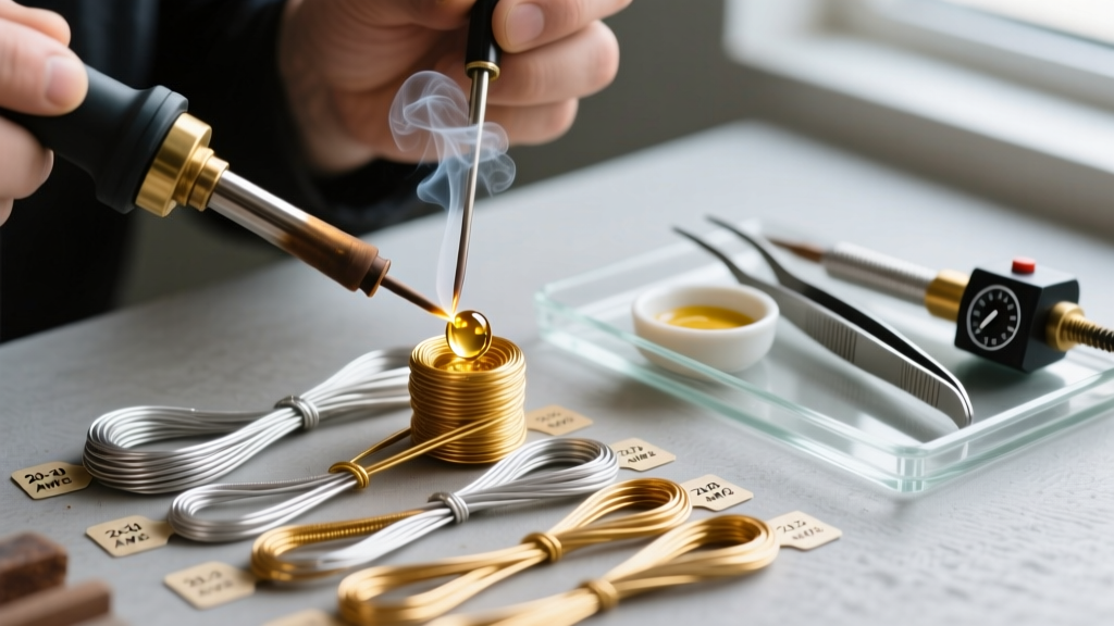
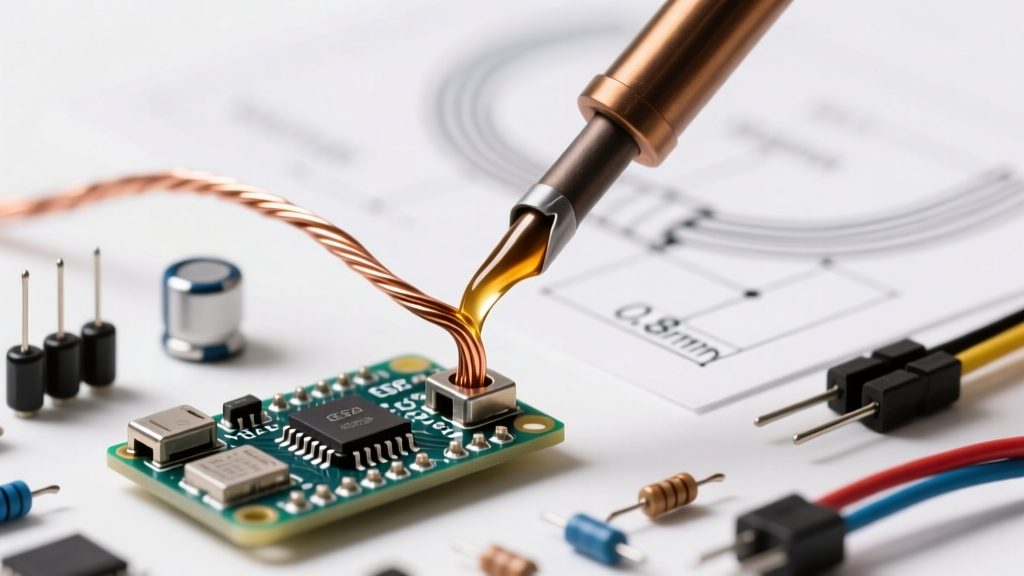
[Camera: Extreme Close-Up, 100mm Macro Lens] We open on a cross-section of a standard 0.031-inch (0.8mm) diameter copper soldering wire. Notice the hollow channels running through the center. This is the flux core. In 2026, high-reliability DIY and professional builds predominantly rely on multi-core flux designs (typically 2% to 3% by weight) to ensure continuous flux activation as the wire melts.
Alloy Selection Matrix
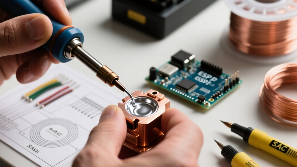
[Overlay: Split-screen comparison] On the left, we have traditional Sn60/Pb40 (Tin/Lead). On the right, the modern lead-free SAC305 (Tin/Silver/Copper). When working specifically with bare copper wire, the thermal conductivity of copper (approximately 401 W/m·K) acts as a massive heat sink.
- Sn60/Pb40 (Leaded): Melts at 183°C (361°F). Visually, it flows like liquid mercury, exhibiting high wetting action and a bright, mirror-like finish. Ideal for beginners and heavy copper wire splicing.
- SAC305 (Lead-Free): Melts at 217°C (423°F). Visually, it appears slightly duller and has a higher surface tension. It requires a more aggressive flux (like RMA or RA) to break through copper oxidation rapidly.
Director's Note: According to the IPC Standards for acceptability, lead-free joints will naturally look grainier and less reflective than leaded joints. Do not mistake a visually dull SAC305 joint for a 'cold' joint if the wetting angle is correct.
[Scene 2] Thermal Dynamics & Profiling
[Overlay: Thermal Imaging Camera (FLIR)] Watch the heat transfer in real-time. When the 350°C iron tip touches the copper pad, the heat doesn't just stay at the point of contact; it rapidly dissipates down the copper trace or wire. If you apply the copper soldering wire too early, the flux boils off before the base metal reaches the melting point, resulting in a charred, non-wetting surface.
Copper Soldering Wire Diameter & Thermal Profile Matrix
| Wire Diameter | Best Use Case | Iron Temp (Sn60/Pb40) | Iron Temp (SAC305) | Max Dwell Time |
|---|---|---|---|---|
| 0.015" (0.4mm) | 0402/0603 SMD, fine pitch | 320°C (608°F) | 350°C (662°F) | 1.5 Seconds |
| 0.031" (0.8mm) | Through-hole, 24-28 AWG wire | 350°C (662°F) | 380°C (716°F) | 2.5 Seconds |
| 0.062" (1.5mm) | Heavy gauge copper, XT60 connectors | 380°C (716°F) | 410°C (770°F) | 4.0 Seconds |
[Scene 3] The Perfect Through-Hole Joint (Slow-Motion Breakdown)
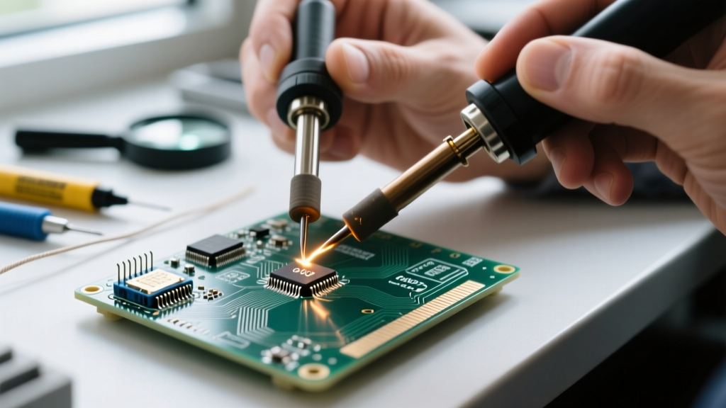
[Action: Slow Motion at 240fps] Let's break down the execution of a flawless copper-to-PCB joint using 0.031" copper soldering wire. We follow the strict thermal sequencing advocated by NASA Workmanship Standards.
- Frame 1 (0.0s): The clean, tinned chisel tip makes contact with both the copper component lead and the PCB pad simultaneously. The iron is held at a 45-degree angle.
- Frame 2 (1.0s): Heat transfers into the copper. The flux from the previous tinning activates, cleaning microscopic oxides.
- Frame 3 (1.5s): The copper soldering wire is introduced to the joint, not the iron tip. As the wire touches the heated copper lead, it instantly flashes into a liquid state, drawn into the barrel via capillary action.
- Frame 4 (2.0s): A concave fillet forms. The solder wets the copper lead, climbing up the wire at a smooth 30-to-45-degree angle.
- Frame 5 (2.5s): The wire is removed first, followed by the iron. The joint cools naturally, forming a bright, smooth, concave volcano shape.
[Scene 4] The Metallurgy: Visualizing the Intermetallic Layer
[Camera: Electron Microscope Render Overlay] What you cannot see with the naked eye is the intermetallic compound (IMC) layer. When molten tin in your copper soldering wire meets the solid copper lead, a metallurgical reaction occurs, forming a Cu6Sn5 (eta phase) layer.
This layer is the actual 'glue' of the solder joint. However, if you exceed the recommended dwell time (e.g., holding the iron for 6+ seconds), the Cu6Sn5 layer grows too thick and transitions into the Cu3Sn (epsilon phase). Visually, the joint might look fine on the outside, but internally, this thick IMC layer is highly brittle. A simple mechanical tug on the copper wire will cause the joint to fracture cleanly at the IMC boundary, leaving a dull, grainy copper surface exposed.
[Scene 5] Macro Troubleshooting: Identifying Visual Defects
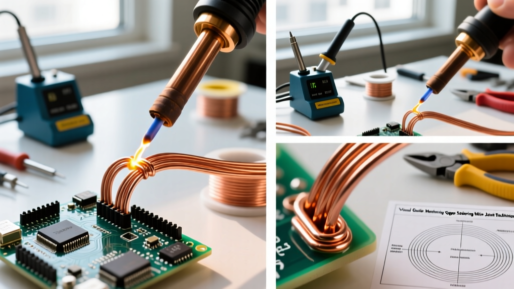
[Overlay: Side-by-Side Macro Comparisons] Let's freeze-frame on three common failure modes when using copper soldering wire, and how to correct them visually.
1. The 'Icicle' or 'Grape' Joint
Visual Cue: The solder balls up on the copper wire but refuses to flow onto the PCB pad, looking like a grape resting on a surface.
The Fix: This is a classic flux starvation and temperature deficit issue. The copper wire acted as a heat sink, dropping the local temperature below the solder's liquidus point before wetting could occur. Remove the joint, apply external liquid rosin flux, and reheat with a wider chisel tip to increase thermal mass transfer.
2. The Disturbed (Frosted) Joint
Visual Cue: The joint has a frosted, cracked, or wrinkled appearance, resembling crumpled aluminum foil.
The Fix: The copper wire was moved while the solder was in the 'plastic' (semi-solid) phase between liquidus and solidus temperatures. This physically tore the forming crystalline matrix. Reheat fully until the solder is completely liquid, hold the wire dead still, and remove the heat.
3. Solder Wicking (The Starved Barrel)
Visual Cue: The solder climbs entirely up the copper component lead, leaving the bottom of the PCB pad bare and dry.
The Fix: The iron tip was placed too high on the component lead rather than at the intersection of the pad and the lead. Heat rises, and the solder followed the heat source. Always apply the iron tip at the exact intersection point, feeding the copper soldering wire from the opposite side.
Director's Cut: 2026 Pro-Tips for Copper Soldering
As component densities increase and DIYers tackle more complex robotics and IoT builds, mastering your consumables is non-negotiable. Always store your copper soldering wire in a sealed, moisture-free environment. Oxidation on the exterior of the wire spool will cause the solder to 'spit' and pop as the surface oxides are violently reduced by the core flux upon melting. For the most comprehensive visual examples of acceptable versus defective solder joints, we highly recommend studying the Adafruit Guide to Excellent Soldering, which pairs beautifully with the thermal theories outlined in this visual masterclass.
[Fade to Black] Remember: soldering is a visual language. Learn to read the flow, respect the thermal mass of copper, and let the flux do the heavy lifting.