
The Metallurgy of Soldering PCB Assemblies: Why Defects Occur
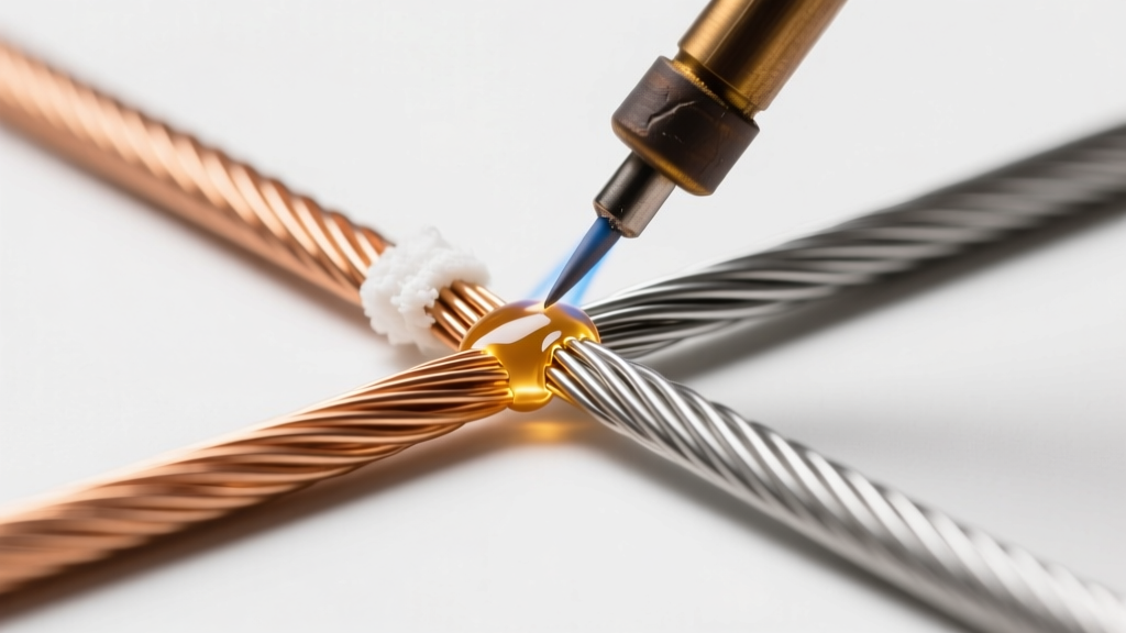
When soldering PCB assemblies, you are not merely gluing components to a board; you are facilitating a complex metallurgical reaction. A successful joint relies on the formation of an Intermetallic Compound (IMC) layer—typically Cu6Sn5 and Cu3Sn—between the copper pad and the tin-based solder alloy. If the thermal profile is incorrect, or if oxidation interferes, this IMC layer fails to form properly, resulting in latent electrical failures. According to the IPC-A-610 Acceptability of Electronic Assemblies standard, even visually marginal joints can compromise the long-term reliability of Class 2 and Class 3 electronics. This guide provides actionable, deep-level troubleshooting protocols for the most common defects encountered when soldering PCB components.
Diagnostic Matrix: Identifying Soldering PCB Defects
Before applying heat, accurately diagnose the failure mode. Use this matrix to cross-reference your visual inspection with the root cause.
| Defect Type | Visual Symptom | Primary Root Cause | IPC-A-610 Status |
|---|---|---|---|
| Cold Joint | Dull, grainy, convex (beaded) surface; poor wetting | Insufficient thermal transfer, lack of flux, premature cooling | Reject (All Classes) |
| Solder Bridge | Solder connects adjacent pads or traces unintentionally | Excessive solder volume, inadequate flux, incorrect tip geometry | Reject (All Classes) |
| Disturbed Joint | Frosty, cracked, or wrinkled appearance; fractured IMC | Component movement during the solidification phase | Reject (All Classes) |
| Pad Lift | Copper pad separated from the FR-4 substrate | Excessive dwell time (>3s), mechanical prying, high iron temp | Reject (Defect) |
Deep Dive 1: Rescuing Cold Solder Joints
A cold solder joint occurs when the solder melts, but the copper pad and component lead do not reach the alloy's liquidus temperature. For standard Sn63/Pb37 eutectic solder (melting point 183°C), the pad must reach at least 215°C to achieve a proper wetting angle of less than 90 degrees. For lead-free SAC305 (melting point 217°C), the pad must exceed 245°C. If the pad is starved of heat, the solder simply sits on top of the oxidation layer, creating a high-resistance, mechanically weak 'grape' joint.
Step-by-Step Cold Joint Rework Protocol
- Clean the Area: Scrub the joint with 99% Isopropyl Alcohol (IPA) and a lint-free swab to remove surface contaminants.
- Apply Fresh Flux: Liquid rosin flux (e.g., Kester 951) or a no-clean tacky flux (e.g., Amtech NC-559-V2-TF) is mandatory. Do not rely on the flux core inside your solder wire for rework; it has likely already been depleted.
- Optimize Tooling: Use a high-thermal-mass chisel tip, such as the Hakko T18-D12. Avoid conical tips, which suffer from poor thermal transfer due to minimal surface area contact.
- Set Precise Temperatures: Configure your station (e.g., Hakko FX-888D, approx. $115) to 350°C for leaded alloys or 380°C for SAC305 lead-free alloys.
- Execute the Heat Transfer: Place the flat of the chisel tip so it touches both the PCB pad and the component lead simultaneously. Hold for exactly 1.5 to 2 seconds.
- Feed and Reflow: Feed Kester 44 rosin-core solder into the pad-lead junction (not directly onto the iron tip). Once the solder flows smoothly and forms a concave fillet, remove the solder wire, then the iron.
Deep Dive 2: Eliminating Solder Bridges on Fine-Pitch ICs
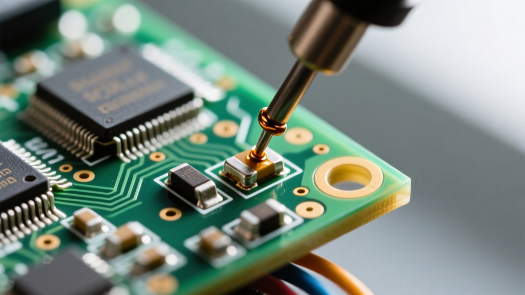
Solder bridges are the most frequent defect when soldering PCB surface-mount components like QFP, SOIC, or QFN packages with 0.5mm to 0.8mm pitches. Bridges occur when surface tension is overcome by excessive solder volume, or when flux boils off too quickly during drag soldering, leaving the molten alloy free to flow across adjacent pads.
The Capillary Wick Removal Method
Attempting to 'drag' the bridge away with a bare iron usually results in smeared solder and damaged pads. Instead, leverage capillary action using high-purity copper desoldering braid. The NASA Workmanship Standard for Soldered Electrical Connections strictly outlines the proper use of wicking to prevent thermal damage to micro-traces.
- Select the Correct Braid Width: For 0.5mm pitch ICs, use Chemtronics Soder-Wick #2 (blue label, 0.060 inch width, approx. $8 per spool). Using a braid that is too wide will wick solder away from the actual pads, creating starved joints.
- Pre-Flux the Braid: Copper oxidizes rapidly when heated. Coat the tip of the braid with a generous layer of Amtech NC-559-V2-TF tacky flux. This lowers the surface tension and accelerates capillary flow.
- Apply Heat: Place the fluxed braid directly over the solder bridge. Press your soldering iron (fitted with a micro-pencil or micro-chisel tip) onto the top of the braid. Set the iron to 360°C.
- Observe the Flow: Within 1 to 2 seconds, you will see the molten solder wick upward into the copper mesh. The moment the bridge clears, lift the iron and braid away simultaneously.
- Final Cleanup: Inspect under 10x magnification. Clean the area with IPA and a soft-bristle ESD-safe brush to remove flux residue that could cause electrochemical migration (dendrite growth) over time.
Expert Callout: The 'Solder Sucker' Warning
Never use a manual or automatic solder sucker (desoldering pump) on fine-pitch SMD pads. The mechanical shockwave generated by the plunger release is more than enough to shear micro-traces or lift delicate BGA pads off the FR-4 substrate. Reserve solder suckers exclusively for heavy-duty through-hole components with large thermal masses.
Deep Dive 3: Mitigating Pad Lifting and Thermal Damage
The FR-4 fiberglass-epoxy substrate used in 95% of commercial PCBs has a Glass Transition Temperature (Tg) typically ranging from 130°C to 170°C. When you apply a 380°C soldering iron to a copper pad, the heat conducts through the trace and into the substrate. If the dwell time exceeds 3 to 4 seconds, the epoxy resin softens, delaminates, and the copper pad lifts away from the board. Once a pad is lifted, the mechanical integrity of the circuit is permanently compromised.
Repairing a Lifted Pad
If you have accidentally lifted a pad during rework, do not panic. You can restore functionality using a jumper wire technique, provided the underlying trace is still intact.
- Secure the Lifted Pad: Clean the area thoroughly. Apply a small drop of specialized PCB epoxy (e.g., CircuitWorks CW2400 or Loctite 401 cyanoacrylate) under the lifted pad and press it flat against the substrate. Allow it to cure fully (typically 10-15 minutes).
- Expose the Trace: Using a fiberglass scratch pen, gently scrape away the solder mask from the trace leading up to the damaged pad, exposing about 2mm of bare copper.
- Install the Jumper: Cut a piece of 30 AWG Kynar-insulated wire-wrap wire. Strip 2mm from one end and solder it directly to the exposed trace. Route the wire over the damaged pad area and solder the other end directly to the component lead.
- Conformal Coating: Once the electrical connection is verified with a multimeter, apply a UV-curable solder mask pen or acrylic conformal coating over the jumper wire to prevent future short circuits and mechanical snagging.
Tooling Maintenance: The Hidden Variable in PCB Soldering
Many technicians blame their solder or flux when the actual culprit is an oxidized iron tip. An oxidized tip acts as a thermal insulator, dropping the effective heat transfer by up to 60%. To maintain peak performance when soldering PCB assemblies, adhere to these maintenance rules:
- Never Use a Wet Sponge: Dipping a 380°C iron tip into a wet cellulose sponge causes rapid thermal shock, leading to micro-fractures in the iron's chrome plating. This exposes the underlying copper core to molten solder, which will rapidly dissolve and pit the tip.
- Use Brass Wool: Clean your tip using a dry brass wire sponge. This removes oxidation and carbonized flux without dropping the tip temperature.
- Always Tin Before Powering Down: The moment you turn off your soldering station, melt a generous blob of rosin-core solder over the entire working surface of the tip. This sacrificial layer of solder will oxidize instead of the tip's iron plating while it cools, ensuring instant wetting the next time you power up.
By understanding the metallurgical requirements of the IMC layer, utilizing precise thermal profiles, and leveraging capillary physics with the right flux and wicking materials, you can systematically eliminate defects. For further reading on advanced desoldering braid techniques and material science, refer to the Chemtronics Soder-Wick Desoldering Braid Technical Guide. Mastery of these troubleshooting protocols will elevate your soldering PCB skills from hobbyist to professional-grade reliability.