
The Physics of the Perfect Joint: Beyond the Basics
In 2026, the market is flooded with advanced smart irons like the Pinecil V2 and FNIRSI HS-01, featuring rapid thermal recovery and USB-C PD power delivery. Yet, the fundamental physics of using a soldering iron to create a reliable electrical and mechanical bond remains unchanged. A perfect through-hole solder joint is not merely melted metal cooling on a pad; it is a carefully controlled metallurgical event.
When you apply heat, you are facilitating the creation of an Intermetallic Compound (IMC) layer—typically Cu6Sn5 when using tin-based solders on copper pads. The ideal IMC layer is between 1 and 2 microns thick. If your dwell time is too short, the IMC layer fails to form, resulting in a weak mechanical bond. If your dwell time is excessive, the IMC layer grows too thick and becomes brittle, prone to micro-fracturing under thermal cycling or mechanical shock.
Expert Insight: According to the IPC-A-610 standard for electronic assemblies, a proper through-hole joint must exhibit excellent wetting, a smooth concave fillet, and complete hole fill (typically 75% to 100% depending on the class of the PCB). Visual inspection is your first line of defense against latent field failures.
Temperature Profiling and Alloy Selection
One of the most common mistakes when using a soldering iron is treating the temperature dial as a volume knob. Higher temperatures do not equal faster soldering; they equal accelerated oxidation and damaged FR-4 epoxy. The correct approach is to match the iron's set temperature to the solder alloy's liquidus point, plus a thermal offset for the mass of the component.
Alloy-Specific Temperature Matrix
| Solder Alloy | Composition | Iron Set Temp | Max Dwell Time | Recommended Flux Type |
|---|---|---|---|---|
| Sn63/Pb37 (Eutectic) | 63% Tin, 37% Lead | 315°C - 330°C | 2.0 - 3.0 seconds | Rosin Mildly Activated (RMA) |
| SAC305 (Lead-Free) | 96.5% Sn, 3% Ag, 0.5% Cu | 350°C - 370°C | 1.5 - 2.5 seconds | No-Clean or Water-Soluble |
| Sn99.3/Cu0.7 | 99.3% Tin, 0.7% Copper | 360°C - 380°C | 1.5 - 2.5 seconds | High-Activity No-Clean |
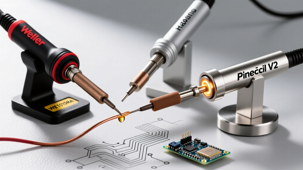
For general prototyping in a well-ventilated home lab, Sn63/Pb37 remains the gold standard due to its low melting point (183°C) and bright, easy-to-inspect joints. However, for commercial or RoHS-compliant builds, SAC305 is mandatory. When using SAC305, you must use a station with high thermal mass and rapid recovery, such as the Weller WE1010NA ($135) or Hakko FX-888D ($110), to prevent the joint from stalling during the phase change.
The 4-Step Execution Sequence
As detailed in SparkFun's comprehensive soldering guide, the physical sequence of applying heat and solder dictates the capillary action that pulls the solder through the plated through-hole (PTH). Do not deviate from this sequence.
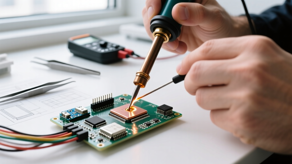
- The Thermal Bridge (0.0s - 0.5s): Place the iron's tip so it simultaneously contacts the component lead and the copper pad. You are heating both surfaces, not the solder. Use a chisel tip (e.g., Hakko T18-D24) to maximize surface area contact.
- Flux Activation & Feed (0.5s - 1.5s): Touch the solder wire to the opposite side of the iron tip, directly where the lead meets the pad. The flux core (e.g., Kester 245) will activate, boiling off oxides and reducing surface tension. The solder will instantly melt and wick into the joint via capillary action.
- Reflow & Wetting (1.5s - 2.5s): Feed exactly enough solder to form a concave fillet. For a standard 0.031" (0.8mm) diameter wire, this is usually 1.5 to 2 inches of wire per joint. Watch the solder flow up the lead and into the barrel of the hole.
- The Withdrawal Sequence (2.5s - 3.0s): This is where amateurs fail. You must remove the solder wire first, followed by the iron tip a fraction of a second later, pulling the tip slightly upward to draw the fillet to a smooth peak. Removing the iron first leaves a dull, disturbed joint.
Flux Chemistry: The Unsung Hero
You cannot successfully master using a soldering iron without understanding flux. Flux is a chemical reducing agent that prevents oxidation at high temperatures. In 2026, the market offers highly specialized formulations:
- Rosin Mildly Activated (RMA): Best for leaded solder. Leaves a hard, amber residue that is generally non-corrosive but can trap moisture if not cleaned with 99% Isopropyl Alcohol (IPA).
- No-Clean Flux: Formulated to leave a minimal, clear residue that is electrically insulating. Ideal for SAC305 and high-density boards where cleaning under components is impossible. MG Chemicals 8341 is a top-tier liquid no-clean flux for rework.
- Water-Soluble (Organic Acid): Extremely aggressive. Provides beautiful, bright joints but must be cleaned with distilled water immediately, or it will cause severe dendritic growth and short circuits over time.
Troubleshooting Common Failure Modes
Even experienced engineers encounter defects. Here is how to diagnose and correct the most common issues when using a soldering iron on through-hole boards.
1. The Disturbed Joint
Symptoms: The joint has a dull, grainy, or frosty appearance, often with a visible ridge around the base.
Root Cause: The component or wire moved during the critical plastic-to-solid phase transition (the eutectic freeze). For 63/37 solder, this happens at exactly 183°C.
Correction: Re-apply flux, reheat the joint fully until the solder flows shiny, hold the component dead still with tweezers or a third-hand tool, and allow it to cool naturally. Never blow on the joint to cool it.
2. Pad Lifting and Delamination
Symptoms: The copper pad separates from the fiberglass FR-4 substrate, sometimes pulling the plated barrel out of the hole entirely.
Root Cause: Excessive dwell time (usually >4 seconds) or excessive iron temperature (>400°C). The epoxy resin in the PCB has a Glass Transition Temperature (Tg) typically around 130°C-150°C; prolonged localized heat destroys the adhesive bond.
Correction: The pad is ruined. You must scrape the solder mask off the connected trace, wrap the component lead around the exposed copper, and solder directly to the trace (creating a dead-bug style repair).
3. Icicle Joints and Poor Wetting
Symptoms: The solder forms a bulbous, convex ball that clings to the lead but does not flow onto the pad.
Root Cause: Insufficient heat transferred to the pad, or severe oxidation on the copper pad preventing wetting. The Adafruit Guide to Excellent Soldering frequently highlights this as a symptom of using a dirty tip or insufficient flux.
Correction: Clean the pad with fiberglass scratch pen or fine sandpaper, apply external liquid flux (like Kester 186), and use a larger chisel tip to increase thermal transfer to the ground plane.
Advanced Tip Maintenance and Longevity
The tip of your soldering iron is a complex piece of engineering: a copper core for thermal conductivity, plated with iron to resist solder erosion, and finished with a micro-layer of tin. How you maintain this tip dictates its lifespan.
Stop using wet sponges. Wiping a 350°C tip on a damp cellulose sponge causes rapid thermal shock. Over time, this micro-cracks the iron plating, allowing the molten solder to eat through to the copper core, destroying the tip in weeks. Instead, use a dry brass wire sponge. It cleans oxidation without dropping the tip's temperature, preserving the thermal recovery cycle of your station.
Always finish your soldering session by applying a thick layer of cheap, high-flux solder (often called 'sacrificial solder') to the tip before turning off the station. This prevents ambient oxygen from reacting with the hot iron plating as it cools down, ensuring your tip is pristine and ready for your next project.