
The Metallurgical Anatomy of Modern Soldering Pencil Tips
When professionals and advanced hobbyists evaluate soldering pencil tips in 2026, the focus has fundamentally shifted from raw station wattage to the microscopic metallurgy and thermal geometry of the tip itself. A soldering tip is not merely a shaped piece of metal; it is a highly engineered thermal conduit designed to transfer Joules of heat into a solder joint while resisting extreme chemical corrosion.
At the core of nearly every high-quality soldering pencil tip lies Electrolytic Tough Pitch (ETP) copper. ETP copper is selected for its exceptional thermal conductivity, which sits at approximately 385 W/(m·K). This allows heat to travel rapidly from the heating element to the working face. However, bare copper dissolves rapidly when exposed to molten tin-lead and lead-free alloys like SAC305 (Tin-Silver-Copper). To combat this, manufacturers apply a complex multi-layer electroplating process.
The Plating Matrix: Iron, Chromium, and Tin
The working face of the tip is coated with an electroplated iron layer, typically ranging from 100 to 150 microns in thickness for standard tips, and up to 300 microns for heavy-duty thermal mass tips. This iron layer has a hardness of roughly 200-300 HV (Vickers Hardness) and acts as a sacrificial barrier against solder dissolution. Behind the iron layer, a microscopic chromium or nickel barrier is often applied to prevent molten solder from creeping up the non-working areas of the tip via capillary action. Finally, the working face is pre-tinned with a thin layer of solder to prevent immediate oxidation during storage and shipping.
Geometry and Thermal Transfer Matrix
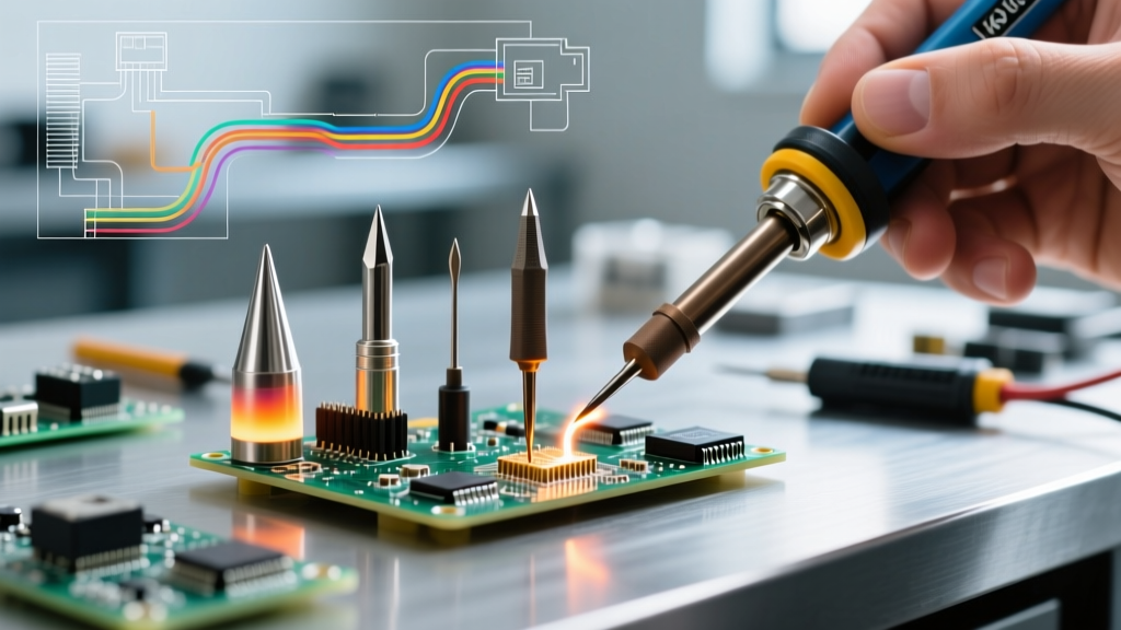
The physical shape of soldering pencil tips dictates both the surface area contact and the thermal mass available to the joint. Selecting the wrong geometry is the leading cause of cold solder joints and damaged PCB pads. Below is a technical breakdown of common geometries and their optimal use cases.
| Tip Geometry | Series Code (Typical) | Thermal Transfer Efficiency | Optimal Application | Limitations |
|---|---|---|---|---|
| Conical (Point) | B-Series / I-Series | Low (Poor surface contact) | Micro-SMD (0201/01005), fine-pitch rework | Struggles with ground planes; high risk of pad lifting due to prolonged dwell time. |
| Chisel (Flat) | D-Series | High (Maximum surface area) | Through-hole, standard 0603/0805 SMD, wire tinning | Difficult to navigate tight component clearances. |
| Bevel (Scoop) | C-Series | Medium-High | Drag soldering SOIC/QFP, holding solder blobs | Requires precise angle control; prone to bridging if overloaded. |
| Knife (Blade) | K-Series | Variable (Edge vs. Flat) | Vertical joints, mixed-technology boards, scraping oxidation | Asymmetric heat distribution can cause uneven wetting on large pads. |
According to the IPC soldering standards, maximizing the contact area between the tip and the lead/pad is critical for achieving proper intermetallic compound (IMC) formation without exceeding the thermal degradation threshold of the component. A 2.4mm chisel tip will transfer heat into a standard 0805 capacitor pad in under 1.5 seconds, whereas a 1.0mm conical tip might require 4+ seconds, drastically increasing the risk of delaminating the PCB's copper trace.
Active vs. Passive Thermal Recovery Dynamics
The evolution of soldering pencil tips is deeply tied to the heater technology they interface with. In 2026, the market is distinctly divided into passive and active tip architectures, each with vastly different thermal recovery profiles.
Passive Tips (e.g., Hakko T18 Series)
Passive tips slide over a separate ceramic heating element. The thermocouple is located inside the heater, not the tip. Because the thermal sensor is separated from the working face by several millimeters of air and metal, the system experiences a thermal lag. When a passive tip touches a large ground plane, the working face temperature drops instantly, but the station's sensor takes 2 to 4 seconds to register the drop and supply more power. These tips rely on high thermal mass (thicker copper cores) to compensate for the lag. In current markets, standard Hakko T18 tips cost between $9 and $12 each.
Active Cartridge Tips (e.g., JBC C245, Weller RT Series)
Active soldering pencil tips integrate the heater and the thermocouple directly into the cartridge, placing the thermal sensor less than 3mm from the working apex. This architecture allows for sub-2-second thermal recovery. When a JBC C245 tip (priced around $48 to $58 per cartridge) contacts a cold joint, the integrated sensor detects the micro-drop in temperature and triggers the station to deliver a massive, instantaneous pulse of current. This allows technicians to use smaller, lower-thermal-mass tips to solder large ground planes without overheating adjacent components, a paradigm shift documented extensively in modern soldering thermal management guides.
Cataloging Failure Modes: Why Tips Die
Understanding how soldering pencil tips fail is essential for optimizing your consumables budget and ensuring joint reliability. Tips rarely 'wear out' from friction; they fail chemically and metallurgically.
Expert Insight: Over 70% of premature tip failures in production environments are caused by improper cleaning protocols and dry-burn oxidation, not mechanical abrasion. Treating a tip as a consumable rather than a precision instrument is a costly mistake.
- Dry-Burn Oxidation: When a tip is left idle at 380°C without a protective layer of solder, the iron plating reacts with atmospheric oxygen to form iron oxide (Fe2O3 and Fe3O4). This oxide layer is a severe thermal insulator. Once a tip turns blue or black, thermal transfer drops by up to 90%. Never attempt to scrape this oxide off with a knife or sandpaper; you will strip the 150-micron iron layer and expose the copper core, destroying the tip instantly.
- Flux Carbonization: Modern no-clean and rosin-based fluxes contain complex organic resins. When subjected to temperatures above 350°C for extended periods, these resins do not fully volatilize; instead, they carbonize and bake onto the iron plating. This carbon shell prevents molten solder from wetting the tip. According to metallurgical data from Kester's technical soldering documentation, maintaining idle temperatures below 320°C when using highly active fluxes significantly reduces carbon buildup.
- Thermal Shock Micro-Cracking: Quenching a 400°C tip into a wet cellulose sponge causes an instantaneous temperature drop of 50°C to 100°C. This rapid thermal contraction induces micro-fractures in the rigid iron plating. Molten solder then penetrates these microscopic cracks, dissolving the underlying copper core and causing the tip to pit and hollow out from the inside.
The 2026 Maintenance Protocol for Maximum Lifespan
To maximize the ROI on premium soldering pencil tips, adopt the following step-by-step maintenance protocol. This routine is designed to preserve the iron plating integrity while ensuring optimal wetting for every joint.
- Switch to Brass Wool: Discard wet cellulose sponges. Use high-quality brass or copper wire shavings (brass wool). Plunging a hot tip into brass wool drops the surface temperature by only 10°C to 15°C, avoiding thermal shock while effectively scraping away oxidized solder and carbonized flux.
- The 'Leave a Blob' Rule: Before placing the iron back in its holder, always melt a generous amount of fresh, flux-cored solder onto the working face. This sacrificial blob acts as an oxygen barrier. The next time you pick up the iron, wipe the oxidized sacrificial blob into the brass wool, revealing a perfectly tinned, pristine working surface underneath.
- Optimize Idle Temperatures: Utilize your station's sleep/auto-standby features. If you are stepping away for more than three minutes, drop the station temperature to 150°C or utilize an auto-off function. Keeping a tip at 380°C while idle accelerates iron oxidation exponentially compared to a 250°C idle state.
- Use Tip Tinner/Activator for Mild Oxidation: If you notice slight de-wetting (solder pulling away from the edges of the tip), do not increase the heat. Instead, plunge the hot tip into a commercial tip tinner (a mixture of mild organic acids and solder powder) for 2-3 seconds, then immediately wipe it on brass wool and apply fresh solder. This chemically reduces light oxidation without damaging the iron plating.
Conclusion
Mastering the use of soldering pencil tips requires moving beyond the assumption that 'hotter is better.' By understanding the metallurgical limits of iron plating, selecting the correct geometric profile for your specific PCB pad sizes, and leveraging active thermal recovery systems, you can achieve flawless intermetallic bonds while extending the lifespan of your consumables by a factor of three or more. Whether you are drag-soldering a 0.5mm pitch QFP with a bevel tip or driving heat into a 10-layer motherboard ground plane with a heavy chisel, respecting the physics of the tip is the hallmark of a true professional.