
The Metallurgy of Modern Soldering Iron Tips
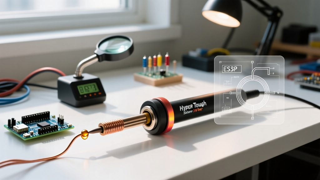
To understand why specific soldering iron tips perform differently on a crowded PCB, you first need to understand their internal architecture. A high-quality tip is not just a piece of metal; it is a precisely engineered thermal conduit. At the core lies a 99.9% pure copper cylinder, chosen for its exceptional thermal conductivity (approximately 400 W/m·K). However, bare copper dissolves rapidly in molten solder, especially when working with aggressive lead-free alloys like SAC305 (Tin-Silver-Copper).
To prevent this, manufacturers electroplate the copper core with a layer of iron, typically between 0.003 and 0.005 inches thick. This iron plating is the actual working surface that contacts the solder. Finally, the sides and rear of the tip are coated with a non-wetting layer of chromium or nickel to prevent solder from creeping up the barrel and oxidizing the heating element. In 2026, with the industry's near-total shift to lead-free assemblies requiring higher working temperatures (330°C to 360°C), the integrity of this iron plating is more critical than ever. Cheap, $2 clone tips often skip the chrome barrier or use microscopically thin iron plating, leading to catastrophic failure within weeks.
Core Comparison Matrix: Shape vs. Thermal Dynamics
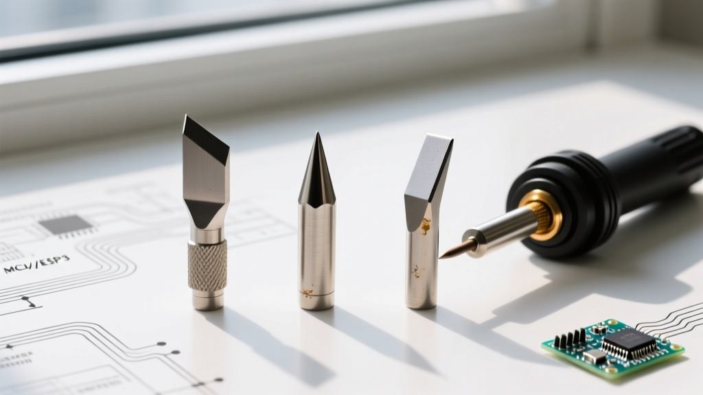
The shape of the tip dictates the surface area contact, which directly governs thermal transfer efficiency. Below is a functional comparison of the three primary geometries used in modern electronics assembly.
| Tip Geometry | Primary Use Case | Thermal Transfer Efficiency | Wetting Surface Area | Skill Level Required |
|---|---|---|---|---|
| Chisel (D-Series) | General purpose, through-hole, 0603 to SOIC-8 | High (Broad flat contact) | Large | Beginner to Expert |
| Conical (B-Series) | Ultra-fine pitch, micro-soldering, 0201 components | Low (Point contact restricts heat flow) | Microscopic | Expert |
| Bevel / Hoof (C-Series) | Drag soldering, tinning thick wires, ground planes | Very High (Solder reservoir effect) | Medium to Large | Intermediate |
Chisel Tips: The Undisputed Workhorse
If you only own one tip, it should be a chisel. The chisel geometry maximizes the physical contact area between the iron and the component lead/pad. According to the principles of thermal dynamics, heat transfer is proportional to the contact surface area. A flat chisel tip bridges the gap between the pad and the lead efficiently, melting SAC305 solder in under two seconds when set to 340°C.
The most common mistake beginners make is buying a chisel tip that is too narrow. A 1.2mm chisel (like the Hakko T18-D12) lacks the thermal mass to handle components connected to internal ground planes, resulting in cold joints. Conversely, a massive 4.0mm chisel (T18-D4) will easily bridge the pins on a 0.8mm pitch SOIC chip.
Top 2026 Chisel Models & Pricing
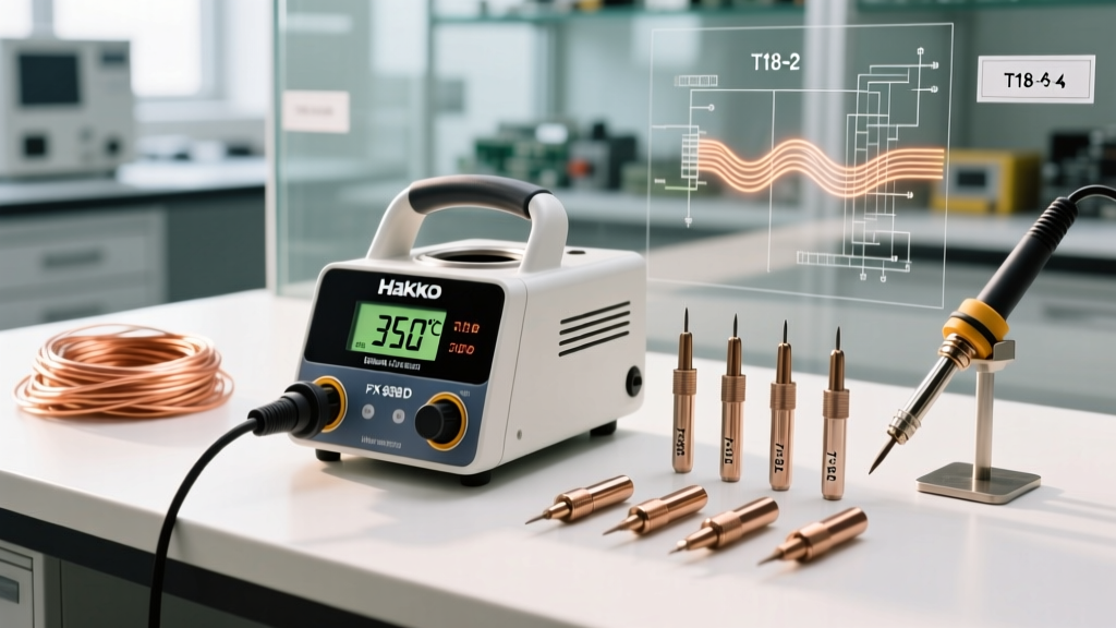
- Hakko T18-D24 (2.4mm): The gold standard for general-purpose SMD and light through-hole work. Priced around $9.50. The 2.4mm width perfectly matches the width of standard SOIC-8 leads without risking bridges.
- Weller ETP (1/16" / 1.6mm): Excellent for tighter spaces and 0603 passives. Priced around $8.00. Features a slightly steeper bevel angle than the Hakko, allowing for better visibility in dense clusters.
- Pine64 Pinecil C4 Tip: A budget-friendly but surprisingly durable option for portable USB-C PD stations, running about $4.50. Great for field repairs where losing a tip isn't financially painful.
Conical Tips: The Precision Trap
There is a pervasive myth in the DIY community that a needle-sharp conical tip is best for fine-pitch surface mount soldering. In reality, conical tips are often the worst choice for standard SMD work due to a severe lack of thermal mass at the apex.
Expert Warning: When a conical tip touches a ground-plane pad, the heat is instantly wicked away into the copper pour. Because the tip's contact area is essentially a microscopic point, the heater cartridge cannot replenish the thermal energy fast enough. The result? You press harder, dwell longer, and ultimately delaminate the PCB pad or destroy the silicon.
Conical tips (such as the Hakko T18-B or Weller ET-B) should be reserved exclusively for micro-soldering tasks where physical clearance is the primary constraint—such as reworking 0201 resistors nestled under RF shields, or performing trace repairs under a high-magnification microscope. For these tasks, the NASA Workmanship Standards Program recommends using the absolute minimum thermal energy required to achieve a wetting angle of less than 90 degrees, which requires immense hand steadiness and specialized micro-soldering stations capable of sub-second thermal recovery.
Bevel and Hoof Tips: Mastering Drag Soldering
Bevel tips (often called hoof tips) are cut at an angle, creating a flat, oval-shaped face that acts as a miniature solder crucible. This geometry is the undisputed king of drag soldering multi-pin ICs like TQFP-48 or LQFP-64 packages.
The concave nature of the bevel allows the tip to hold a small reservoir of molten solder and flux. As you drag the tip across the pins, the surface tension of the solder naturally pulls it onto the copper pads while the flux breaks the oxidation barrier. The IPC J-STD-001 Standard for soldered electrical assemblies dictates strict criteria for fillet formation and wetting; a properly executed drag solder pass with a bevel tip consistently meets Class 3 (High-Reliability) requirements.
Step-by-Step Drag Soldering Flow with a Bevel Tip
- Prep: Apply a generous amount of no-clean or RMA tacky flux to all pins of the IC. Ensure the chip is aligned.
- Tin the Tip: Melt a moderate bead of 63/37 or SAC305 solder directly onto the bevel face of the T18-C2 (2.0mm) tip.
- The Drag: Tilt the iron to a 45-degree angle. Gently touch the bevel to the pins on one side of the IC and pull slowly (approx. 1mm per second) across the row.
- Cleanup: If bridges form, do not panic. Apply more liquid flux and use a clean, dry chisel tip (or copper wick) to pull the excess solder away.
Failure Modes: Why Tips Degrade in Lead-Free Environments
Even premium soldering iron tips from Hakko, Weller, or JBC are consumables. However, understanding failure modes can extend a tip's lifespan from a few weeks to several years.
- Iron Plating Dissolution: Lead-free solders (Sn-Ag-Cu) are highly aggressive and dissolve the iron plating up to 40% faster than traditional 63/37 leaded solder. Running your station at 400°C to compensate for poor thermal transfer will accelerate this erosion exponentially. Keep lead-free temps below 360°C whenever possible.
- Dry Oxidation (The Black Crust): Leaving a station idle at 350°C without a protective layer of solder causes the iron plating to oxidize into a black, non-wetting crust. Once oxidized, heat transfer drops by over 80%. Always leave a thick blob of solder on the tip before powering down.
- Thermal Shock: Quenching a hot tip in a wet brass sponge or water causes microscopic cracking in the iron plating. Solder then penetrates these cracks, reaches the copper core, and rapidly hollows out the tip from the inside. Use a dry brass wire ball (like the Hakko 599B) for cleaning.
- Mechanical Abrasion: Using the tip as a pry tool, or scraping it aggressively against abrasive fiberglass cleaning pens, will strip the iron plating entirely. For detailed maintenance protocols, refer to the official Hakko Tip Maintenance Guidelines.
Expert Verdict: Building Your 2026 Tip Arsenal
Stop buying 10-piece variety packs from unknown marketplace vendors. Those tips use inferior copper alloys and lack proper chromium barriers, which will quickly oxidize and ruin your station's heating element sleeve. Instead, invest $30 to $40 in three genuine, high-quality tips tailored to your actual workflow.
The Ultimate 3-Tip Starter Kit:
- Hakko T18-D24 (2.4mm Chisel): Your daily driver for 90% of all SMD and through-hole tasks.
- Hakko T18-C2 (2.0mm Bevel): Dedicated exclusively to drag soldering ICs and tinning heavy-gauge wires.
- Hakko T18-B3 (0.8mm Conical): Kept in reserve strictly for microscope-assisted micro-rework and tight-clearance trace jumps.
By matching the geometry of the tip to the thermal demands of the joint, you will produce stronger, shinier, and more reliable solder joints while drastically reducing your consumable costs over the life of your station.