
The Geometry of Heat: Why the Chisel Profile Reigns Supreme
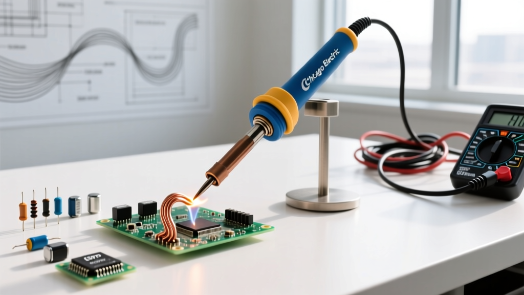
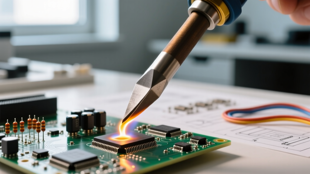
When building or repairing printed circuit boards (PCBs), the soldering iron chisel tip is universally recognized as the workhorse of electronics assembly. Unlike conical tips that terminate in a fine point, the chisel tip features a flattened, beveled edge. This geometric distinction is not merely aesthetic; it fundamentally alters the physics of thermal transfer. By maximizing the surface area in contact with both the component lead and the PCB pad simultaneously, the chisel profile drastically reduces thermal resistance at the joint. According to the IPC J-STD-001 standards for soldered electrical and electronic assemblies, achieving proper wetting and a smooth, continuous fillet requires rapid, uniform heating—a feat the chisel tip accomplishes far more efficiently than its conical counterparts.
Thermal Transfer Dynamics and Wetting Area
The primary failure point for beginners is attempting to use a micro-conical tip on standard through-hole or large SMD components. A conical tip transfers heat via point contact, creating a severe bottleneck for thermal energy. The soldering iron chisel tip, conversely, utilizes line contact. When the flat edge is laid flush against a pad and a lead, the cross-sectional area for heat flow increases exponentially.
The Capillary Action Advantage
Beyond raw heat transfer, the flat geometry of a chisel tip acts as a capillary bridge. When flux is activated and solder is introduced, the molten alloy naturally wicks across the flat surface of the tip and flows directly into the joint via capillary action. As highlighted in the Adafruit Guide to Excellent Soldering, maintaining a clean, tinned surface on a chisel tip creates a liquid thermal bridge that transfers heat roughly 50 times faster than air gaps or dry, oxidized metal surfaces.
Definitive Soldering Iron Chisel Tip Sizing Matrix
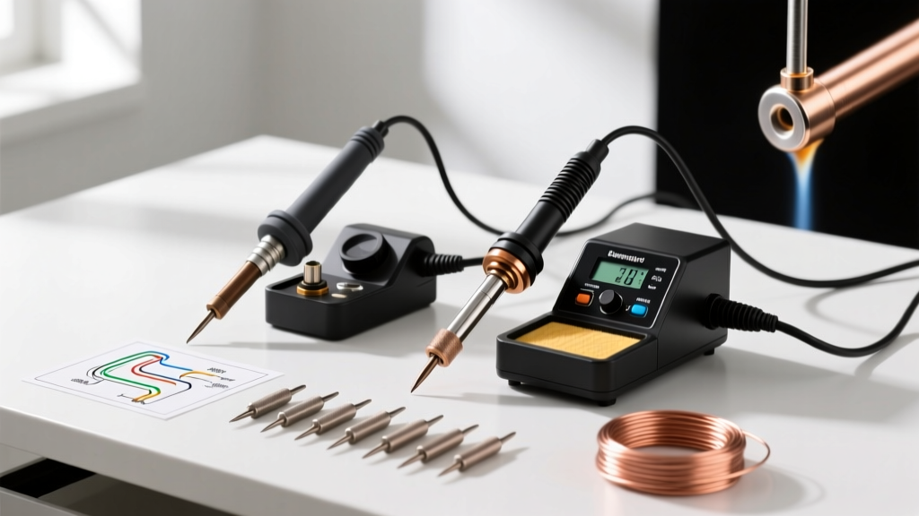
Selecting the correct width for your chisel tip is critical. A tip that is too narrow will lack the thermal mass to heat heavy ground planes, while a tip that is too wide risks bridging adjacent pins on fine-pitch ICs. Below is a comprehensive sizing matrix mapping tip dimensions to specific 2026 assembly scenarios.
| Tip Width (mm / in) | Target Application | Hakko T18 Equivalent | Weller ET Equivalent | Est. Price Range (2026) |
|---|---|---|---|---|
| 1.2mm (3/64") | 0603/0805 SMD, TSSOP, fine drag soldering | T18-D12 | ETS (1/32") | $8 - $12 |
| 2.4mm (3/32") | Standard DIP ICs, 1206 SMD, general through-hole | T18-D24 | ETB (1/16") | $8 - $12 |
| 4.0mm (5/32") | Heavy gauge wire (14-18 AWG), large ground planes | T18-D4 | ETD (1/8") | $9 - $14 |
| 6.0mm (1/4") | Automotive wiring, thick multilayer RF boards | T18-D6 | N/A (Use LT series) | $10 - $15 |
Advanced Application: Drag Soldering Fine-Pitch ICs
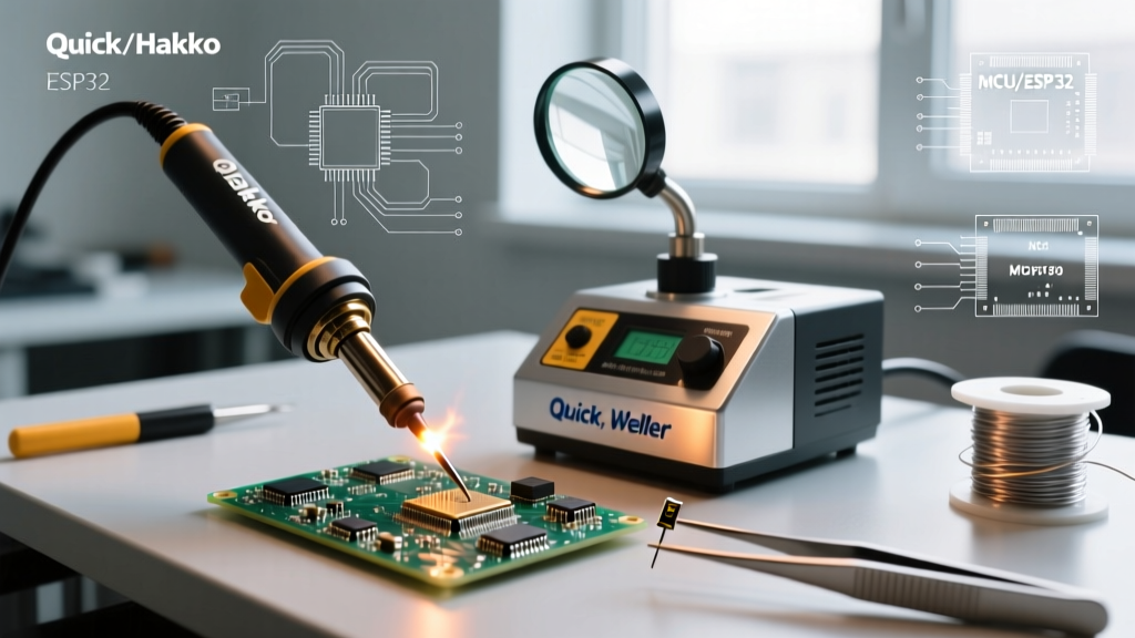
While many associate the chisel profile exclusively with through-hole components, a narrow chisel tip (1.2mm to 1.6mm) is the ultimate tool for drag soldering fine-pitch surface-mount ICs, such as QFP or SOIC packages. The flat edge holds a reservoir of molten solder, allowing you to glide across dozens of pins in seconds.
- Prep and Tack: Apply a thin layer of tacky flux (e.g., Chip Quik SMD291AX) to the pads. Tack two opposing corner pins with a standard iron to align the IC perfectly.
- Load the Tip: Melt a small bead of high-quality rosin-core solder onto your 1.2mm chisel tip. The flux core must be fully activated.
- The Drag: Tilt the iron to roughly 45 degrees. Rest the flat edge of the chisel across the pins and slowly pull the iron from one end of the IC to the other. Let capillary action pull the solder off the tip and onto the fluxed pads.
- Clear Bridges: If solder bridges form between pins, apply fresh liquid flux and drag a clean, dry chisel tip (wiped on brass wool) across the pins. The tip will absorb the excess solder.
- Inspection: Verify fillet formation under a magnifying lamp or digital microscope to ensure compliance with IPC Class 2 or Class 3 standards.
Tackling High Thermal Mass Ground Planes
When soldering components connected to internal copper ground planes on multilayer PCBs, the board acts as a massive heat sink. A common mistake is turning the station temperature up to 400°C+ using a small tip. This instantly oxidizes the tip and damages the PCB's FR4 substrate. As detailed in SparkFun's Through-Hole Soldering Tutorial, the correct approach is to increase the thermal mass of the tip, not the temperature. Switching to a 4.0mm or 6.0mm chisel tip allows you to maintain a safe station temperature of 340°C (for lead-free SAC305) while delivering the sheer joules of energy required to saturate the ground plane and form a reliable metallurgical bond.
Critical Failure Modes: Erosion, Oxidation, and Plating Loss
Modern soldering iron tips are not solid iron. They consist of a highly conductive copper core, plated with a layer of iron to prevent the solder from dissolving the copper, and finished with a microscopic layer of chromium to prevent oxidation on the non-working surfaces. Understanding this metallurgy is key to preventing premature tip death.
- Iron Plating Erosion: Lead-free alloys like SAC305 require higher operating temperatures (340°C–360°C) and utilize highly active carboxylic acid fluxes. This combination attacks the iron plating up to three times faster than traditional Sn60/Pb40 leaded solder. Never leave a lead-free iron idling at 360°C; use sleep mode or turn it off.
- Dry Tip Syndrome: When flux burns onto the working surface of the chisel tip, it forms a hard, black carbon crust. This crust acts as a thermal insulator. Never scrape this off with a steel file or sandpaper, as you will strip the iron plating entirely, ruining the tip instantly.
- Thermal Shock Cracking: Cleaning a 350°C chisel tip on a soaking wet cellulose sponge causes rapid thermal contraction. Over time, this creates micro-fractures in the iron plating, allowing molten solder to reach the copper core and hollow out the tip from the inside. Always use dry brass wire wool for cleaning.
Expert Insight: "The activation temperature of your flux dictates your minimum iron temperature. If you are using a no-clean synthetic flux that activates at 180°C, but your chisel tip is set to 280°C, the flux will burn off before the thermal mass of the joint reaches the solder's liquidus point. Match your tip mass to the joint, and your temperature to the flux chemistry."
2026 Market Standouts: Top Chisel Tip Ecosystems
The market for soldering stations has evolved significantly, with smart stations and advanced cartridge systems leading the charge. Here are the top ecosystems for chisel tips currently dominating the bench:
- Hakko FX-951 / T18 Series: The undisputed standard for professional production environments. The T18-D24 (2.4mm chisel) offers exceptional longevity and costs roughly $9 per tip. The composite heater-sensor design provides rapid thermal recovery.
- JBC C245 Cartridge System: JBC's integrated heater-sensor-thermocouple cartridge design offers zero-delay thermal recovery. The C245-115 and C245-116 chisel profiles are unparalleled for heavy ground plane work, though the $40+ per tip price tag reflects their premium engineering.
- Pine64 Pinecil V2 (D24 Tip): For hobbyists and field technicians, the open-source Pinecil V2 running RISC-V architecture is a revelation. Compatible with TS100-style tips, the D24 chisel tip costs under $6 and delivers 65W of rapid-heating power via USB-C PD.
Frequently Asked Questions
Can I use a chisel tip for 0402 SMD components?
Yes, but you must use a micro-chisel (1.0mm or 1.2mm width). Standard 2.4mm chisel tips will easily bridge the 0.5mm gap between 0402 pads. Ensure your iron has precise low-wattage control to prevent blowing the component off the pad with excessive convective heat.
Why does my chisel tip turn black immediately after tinning?
This is rapid oxidation, usually caused by one of three factors: your station temperature is set too high (above 380°C), you are using cheap solder with highly corrosive flux, or you are wiping the tip on a damp sponge without immediately applying fresh solder to re-seal the iron plating. Always leave a thick blob of sacrificial solder on the tip when powering down.