
The Metallurgical Reality of Lead-Free Alloys
Transitioning from traditional tin-lead (Sn63/Pb37) to RoHS-compliant lead-free alloys is one of the most significant hurdles in modern electronics assembly. When selecting a soldering iron for lead free solder, the primary challenge is not merely the higher melting point; it is the fundamental change in metallurgical behavior. Lead acts as a surfactant in traditional solder, drastically lowering surface tension and promoting rapid wetting. Without lead, alloys like SAC305 (Tin-Silver-Copper) exhibit high surface tension, resulting in sluggish flow, increased oxidation, and a higher propensity for cold or disturbed joints.
According to Wikipedia's comprehensive breakdown of lead-free alloys, the most common lead-free variants require precise thermal management to prevent component damage while ensuring adequate intermetallic compound (IMC) formation. If your thermal delivery is inadequate, the solder will ball up, refuse to wet the pad, or form a grainy, unreliable joint.
Common Lead-Free Alloys and Their Characteristics
| Alloy Designation | Composition | Melting Point (°C) | Wetting & Flow Characteristics |
|---|---|---|---|
| Sn63/Pb37 (Reference) | 63% Sn, 37% Pb | 183°C (Eutectic) | Excellent, fast flow, shiny finish |
| SAC305 | 96.5% Sn, 3.0% Ag, 0.5% Cu | 217°C - 220°C | Sluggish, high surface tension, dull finish |
| SN100C | 99.3% Sn, 0.7% Cu, Ni/Ge | 227°C | Cost-effective, good wetting, very dull |
| SAC0307 | 99.0% Sn, 0.3% Ag, 0.7% Cu | 217°C - 225°C | Lower silver cost, slightly reduced drop-shock resistance |
Why Wattage and Sensor Placement Matter More Than Peak Temperature
A common and destructive mistake among hobbyists and junior technicians is attempting to compensate for the poor wetting of lead-free solder by cranking a low-wattage iron to 400°C or higher. This approach guarantees oxidized pads, lifted traces, and rapid tip destruction. The correct methodology relies on thermal recovery rather than peak temperature.
When a soldering tip contacts a copper ground plane, heat is instantly wicked away. A traditional 40W iron with a remote ceramic heating element and a screw-on tip suffers from severe thermal lag. The sensor reads the heater's temperature, not the tip's working edge. By the time the heater responds, the tip temperature has plummeted below the solder's liquidus point, resulting in a cold joint.
To properly use a soldering iron for lead free solder, you must invest in a station with cartridge-style tips where the heating element and thermocouple are integrated directly into the tip shaft. This reduces thermal mass and sensor distance to near zero.
- JBC CD-2BQF with C245 Handles: Priced around $550-$600, JBC stations deliver 130W of dynamic power. The C245 cartridge tips heat from room temperature to 350°C in under two seconds, providing unmatched thermal recovery for heavy ground planes.
- Weller WX2021 with WXP120: At approximately $650, the Weller WX series utilizes RTW (Rapid Thermal Response) tips. The 120W iron maintains a stable interface temperature even when dragging across multi-layer PCB ground fills.
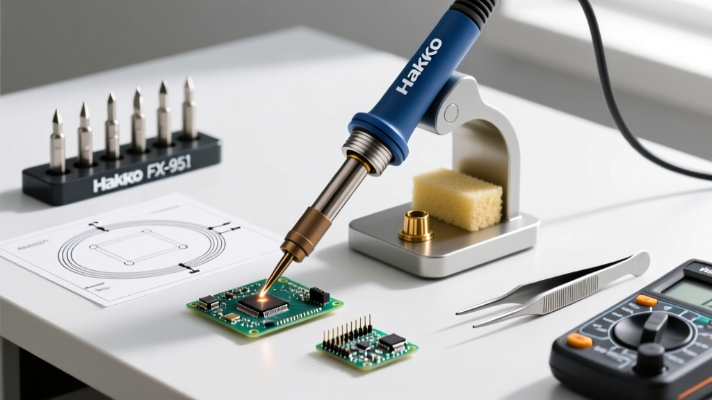
- Hakko FX-951 with T12 Cartridges: A more budget-friendly professional option ($250-$300). The T12 tips offer excellent integrated sensor technology, though the 70W maximum output may struggle slightly with massive copper pours compared to JBC or Weller.
Step-by-Step Technique for Flawless Lead-Free Joints
Mastering the physical technique requires adjusting your muscle memory from the forgiving nature of tin-lead solder. Follow this strict protocol to ensure compliance with the IPC J-STD-001 standard for soldered assemblies.
1. Aggressive Flux Application
Lead-free solder relies entirely on flux to break down the heavy oxide layer that forms instantly at 220°C+. Do not rely solely on the flux core inside your solder wire. Apply an external, highly activated no-clean or RMA (Rosin Mildly Activated) flux paste or liquid—such as Amtech NC-559-V2 or Kester 951—directly to the pad and component lead before applying heat. The flux must be formulated specifically for lead-free temperatures; standard tin-lead fluxes will burn off and carbonize before SAC305 even melts.
2. Optimal Temperature Settings
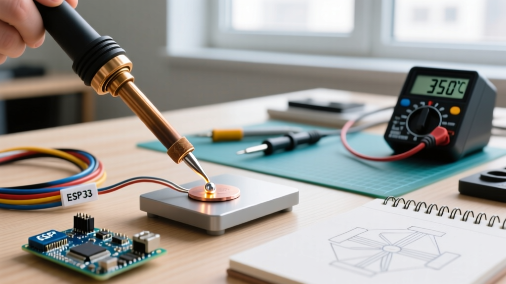
Set your cartridge-based station to 320°C - 350°C. This provides enough thermal headroom to melt the alloy and allow the flux to activate, without exceeding the thermal degradation threshold of most FR-4 laminates and SMD component bodies.
3. The 3-Second Dwell Rule
- Tin the Tip: Apply a small amount of lead-free solder to the clean tip to create a thermal bridge.
- Apply Heat: Place the tinned tip so it simultaneously contacts the PCB pad and the component lead. Hold for exactly 1 to 1.5 seconds to pre-heat the joint.
- Feed the Solder: Apply your 0.5mm or 0.8mm diameter lead-free solder wire to the joint, not the tip. The heat from the pad and lead should melt the wire.
- Withdraw: Once the solder flows and forms a smooth fillet, remove the solder wire, then immediately remove the iron. Total dwell time must not exceed 3 to 4 seconds.
Expert Insight: If the solder refuses to flow after 3 seconds, do not hold the iron there longer. Remove the iron, let the board cool, clean the area with isopropyl alcohol, apply fresh flux, and try again. Prolonged heat application will delaminate the PCB pad.
Combating Tip Erosion and Blackening
Lead-free solder is notoriously hostile to soldering tips. The high tin content (96%+) in SAC305 and SN100C actively dissolves the iron plating on the tip's working edge—a phenomenon known as tin-lead erosion (or more accurately, tin-iron erosion). A tip that would last six months with Sn63/Pb37 may be pitted and ruined in three weeks with lead-free alloys if improperly maintained.
Strict Tip Maintenance Protocol
- Never Dry-Wipe: Avoid using brass wire sponges aggressively. The mechanical abrasion strips the weakened iron plating. Use a high-quality, damp cellulose sponge or a specialized copper wire sponge (like the Hakko 599B) with a light touch.
- Use Chemical Tip Tinner: If your tip develops a black oxide crust that refuses to wet, do not scrape it with a knife or sandpaper. Use a chemical tip tinner/cleaner (such as Edsyn TSC or Kester's technical solder profiles recommended cleaners). Dip the hot tip into the chemical paste for 3 seconds, then wipe on a damp sponge. This chemically reduces the oxide and re-tins the surface simultaneously.
- The Shutdown Blob: Before powering off your station, melt a massive, generous blob of lead-free solder over the entire working surface of the tip. This sacrificial layer will oxidize and erode while the iron is off and cooling, protecting the vital iron plating underneath. Wipe it clean only when you power the station back on for your next session.
Troubleshooting Common Lead-Free Defects
Even with the correct soldering iron for lead free solder, environmental and technique variables can cause defects. Here is how to identify and correct them:
- Grainy or Dull Joints: Unlike the shiny finish of tin-lead, SAC305 and SN100C joints are naturally dull and slightly grainy. However, if the joint looks excessively rough or crystalline, it is a "disturbed joint." This occurs if the component moved while the solder was cooling through its plastic (semi-solid) phase. Clamp the board securely and ensure no vibrations occur during the 2-second cooling window.
- Dewetting (Solder Pulling Away): The solder melts but pulls back from the pad edges, leaving exposed copper. This is almost always caused by oxidized pads or insufficient flux activation. Clean the PCB with a fiberglass scratch pen or isopropyl alcohol, apply a heavy coat of RMA flux, and pre-tin the pad before attempting to solder the component.
- Solder Balling / Grape Graping: Small spheres of solder refuse to coalesce into a single fillet. This indicates that the flux has burned off before the solder reached its liquidus point, leaving oxides on the solder surface. Lower your iron temperature by 10°C, use a more thermally stable no-clean flux, or switch to a slightly larger tip geometry to transfer heat faster without relying on extreme temperatures.
Final Thoughts on Tooling and Technique
Succeeding with lead-free alloys requires abandoning the brute-force heat methods of the past. By investing in a high-thermal-recovery cartridge station, utilizing aggressive lead-free-specific fluxes, and adhering to strict dwell-time limits, you can produce IPC-compliant, highly reliable joints without destroying your PCBs or your equipment. The right soldering iron for lead free solder is ultimately defined by its ability to deliver instantaneous thermal energy exactly where it is needed, keeping the interface temperature stable despite the demanding nature of modern RoHS-compliant metallurgy.