
The Hidden Cost of a Dirty Soldering Iron Tip
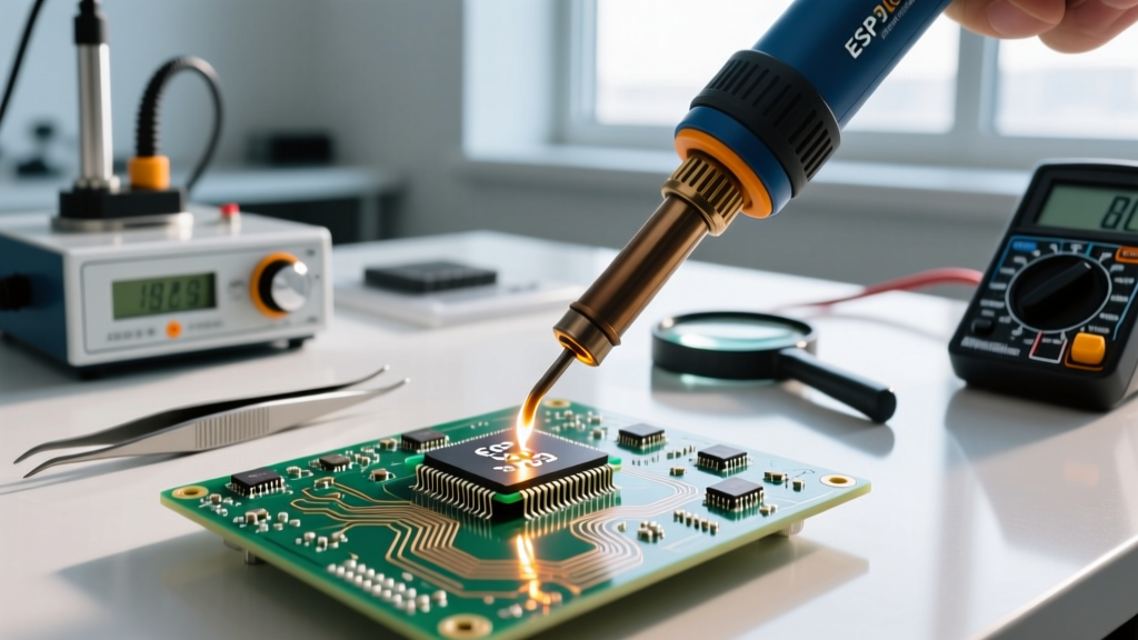
In professional electronics assembly and advanced DIY prototyping, the condition of your soldering iron tip dictates the quality of every single joint. When you need to clean soldering iron tip surfaces, you are not just removing cosmetic blemishes; you are restoring thermal transfer efficiency. A heavily oxidized or carbon-encrusted tip acts as a thermal insulator. This forces the operator to apply excessive pressure or dwell on the pad for too long, ultimately causing lifted traces, damaged component leads, and degraded PCB laminates. According to the IPC guidelines on soldering workmanship, proper thermal management and tip maintenance are foundational to meeting Class 2 and Class 3 reliability standards. Ignoring tip hygiene leads to a vicious cycle of poor wetting, increased flux usage, and premature tip replacement, which can easily cost hobbyists and small labs hundreds of dollars annually in consumable parts.
The Science of Tip Degradation and Oxidation
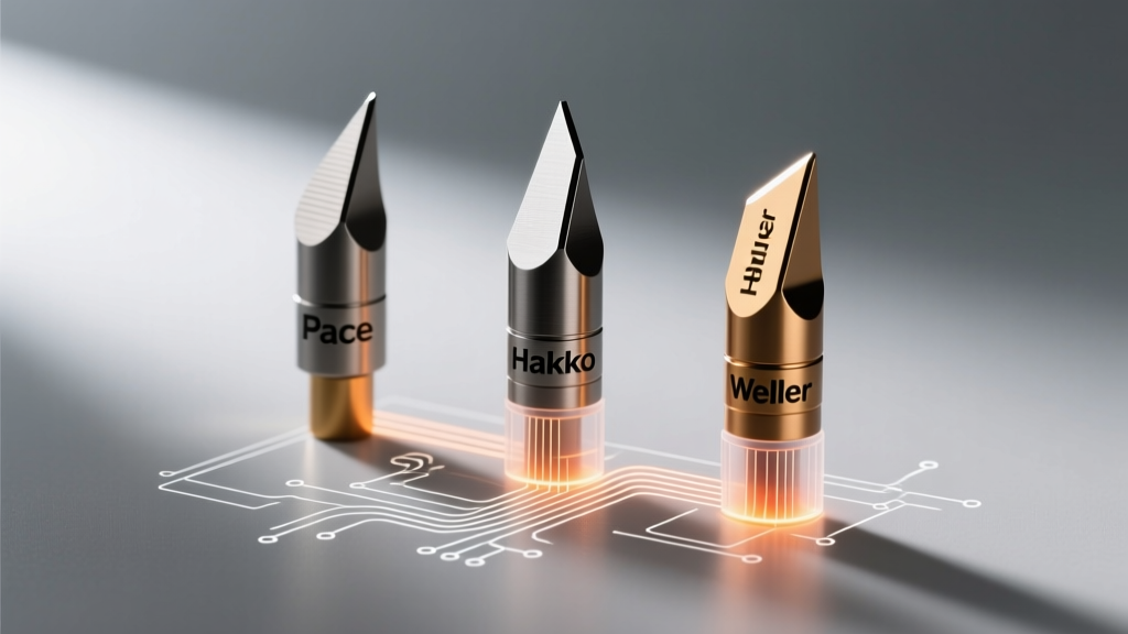
Modern soldering iron tips, such as the ubiquitous Hakko T18 series or the Weller RT1 line, are not solid copper. They are complex, multi-layered structures. The core is high-purity copper for rapid heat transfer, plated with a thin layer of iron (typically 100 to 150 microns thick) to resist erosion from molten solder, and finally finished with a chromium or nickel layer on the non-working surfaces to prevent solder creep. Oxidation occurs when the iron plating reacts with oxygen in the air at elevated temperatures. The rate of this chemical reaction is non-linear. Research from the NASA Electronic Parts and Packaging (NEPP) program highlights that thermal cycling and extreme heat accelerate micro-cracking in the iron plating, allowing oxygen to reach the copper core and cause catastrophic tip failure. Understanding this metallurgy is critical when deciding how to properly clean soldering iron tip surfaces without compromising the delicate iron layer.
Cleaning Mediums Compared: Brass Wool vs. Sponge vs. Chemical
The debate over the best medium to clean soldering iron tip surfaces has persisted for decades. The choice of cleaning material directly impacts the tip's operating temperature and physical integrity. Below is a comparative analysis of the three primary cleaning methods used in modern electronics workstations.
| Cleaning Medium | Thermal Shock | Abrasion Level | Best Use Case | Est. Cost (USD) |
|---|---|---|---|---|
| Brass Wire Wool | Low | Mild Mechanical | Daily maintenance, lead-free alloys, high-temp work | $12 - $18 |
| Cellulose Sponge | High (Severe) | None | Heavy water-soluble flux residue removal | $2 - $5 |
| Chemical Tip Tinner | None | Chemical/Mild Abrasive | Rescuing severely oxidized or blackened tips | $15 - $22 |
Why Experts Prefer Brass Wool
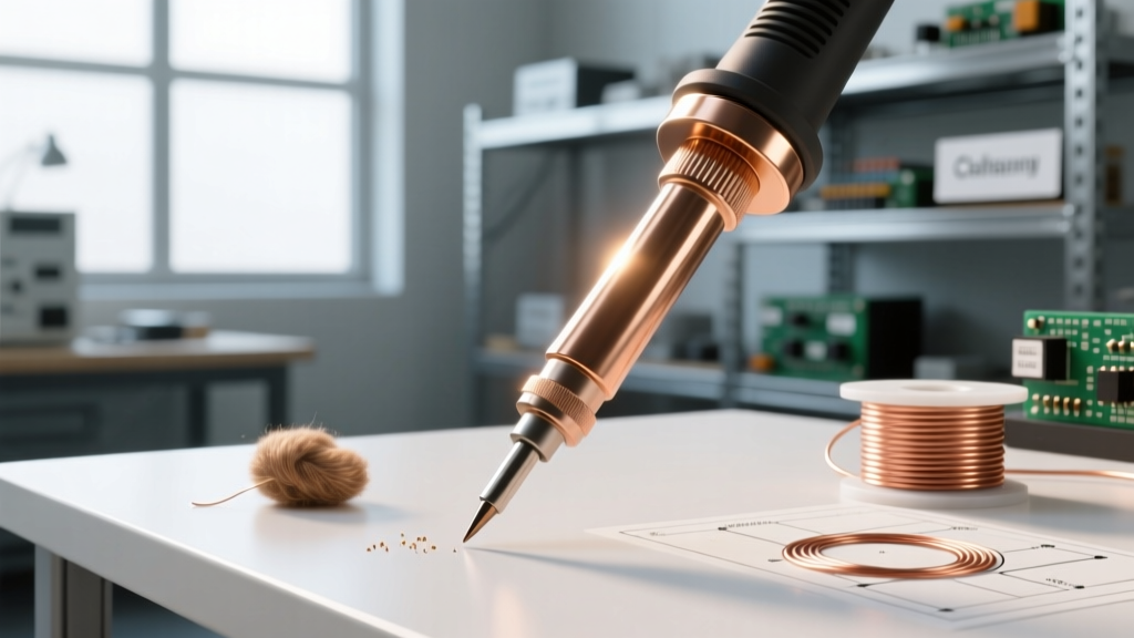
Using a damp cellulose sponge causes a rapid temperature drop of 100°C or more in milliseconds. This severe thermal shock induces micro-fractures in the iron plating. Conversely, a brass wool cleaner (like the Hakko 599B or Weller WDC1 dry cleaner) wipes away oxidized solder and flux carbon without significantly dropping the tip temperature. Brass is softer than the iron plating, meaning it cleans effectively without scratching the working surface. For high-reliability soldering, brass wool is the undisputed industry standard for active cleaning.
The 3-Step Expert Protocol to Clean Soldering Iron Tip Surfaces
To maximize the lifespan of precision micro-tips and heavy-duty chisel tips alike, implement this strict three-phase maintenance protocol.
Phase 1: Pre-Heat and Initial Tinning
- Low-Temperature Start: Never power your station directly to 400°C. Set the dial to 250°C and allow the iron to stabilize. This prevents the flux core in the existing solder from instantly carbonizing before it can protect the tip.
- Feed Solder Immediately: As the tip crosses the melting point of your solder (around 183°C for Sn63/Pb37 or 217°C for SAC305), feed a generous amount of rosin-core solder over the entire working surface.
- Wipe and Inspect: Use your brass wool to gently wipe the tip. The result should be a mirror-like, silver finish. If you see black spots, proceed to the advanced troubleshooting section below.
Phase 2: Active Soldering Maintenance
During active assembly, the rule is simple: wipe, tin, solder, repeat. Before every single joint, wipe the tip in the brass wool to remove the oxidized solder from the previous joint. Immediately apply a tiny amount of fresh solder to the tip before touching the PCB pad. This fresh solder acts as a thermal bridge and a sacrificial oxidation layer. After completing the joint, wipe again and apply a thicker coat of solder to protect the tip while you position the next component.
Phase 3: The Critical Shutdown Sequence
Most tip destruction occurs when the iron is turned off. As the station powers down and the tip cools through the 200°C to 300°C range, oxidation accelerates if the tip is bare. Always leave a massive blob of solder on the tip when shutting down. This sacrificial blob will oxidize instead of the iron plating. When you power up the station for your next session, simply melt and wipe away this dirty blob, revealing a perfectly preserved tip underneath.
Advanced Troubleshooting: Rescuing Severely Oxidized Tips
Even with strict protocols, tips can become oxidized due to accidental idle time or the use of highly active, no-clean fluxes that leave corrosive residues. When standard brass wool fails to clean soldering iron tip surfaces, you must intervene chemically.
Using a Chemical Tip Tinner
Products like the Hakko FS-100 Tip Tinner or MG Chemicals 8341 contain a mixture of solder powder, mild abrasives, and phosphoric acid. To use:
- Set your station to a moderate 300°C.
- Plunge the oxidized tip directly into the tinner paste for 2 to 3 seconds while twisting it slightly.
- The acid will strip the black iron oxide, while the solder powder instantly tins the exposed metal.
- Immediately transfer the tip to your brass wool to wipe away the acidic residue, then apply fresh, high-quality rosin-core solder.
Warning: Do not use sandpaper, files, or fiberglass scratch pens. As detailed in Hakko's official tip maintenance documentation, removing the iron plating via physical abrasion exposes the copper core, which will dissolve into the molten solder within minutes, permanently destroying the tip.
Flux Carbonization and Tip Geometry
Flux carbonization creates a hard, black crust that repels molten solder. This is especially problematic on conical tips (like the T18-B), which have low thermal mass and a tiny surface area. If you frequently struggle with carbon buildup, switch to a chisel tip (such as the T18-D12 or T18-D24). The broader surface area distributes heat more efficiently, allowing you to use lower temperatures and reducing the localized burning of flux residues.
Expert Insight on Lead-Free Alloys: When transitioning to lead-free SAC305 solder, the required tip temperature increases from 350°C to roughly 380°C. Because oxidation rates effectively double for every 10°C increase above 350°C, your tip will degrade up to eight times faster if left untinned. Never leave a lead-free station idle for more than three minutes without a heavy coat of fresh solder on the working end, and consider using a nitrogen-assisted soldering station to displace oxygen around the tip.
Knowing When to Condemn a Tip
No maintenance routine lasts forever. You must know when to discard a tip to prevent damage to your PCBs. Condemn the tip immediately if you observe any of the following failure modes:
- Pitting or Cratering: Visible divots in the working surface caused by prolonged exposure to molten solder leaching the iron plating.
- Copper Exposure: Any sign of a gold or copper color showing through the silver iron layer.
- Asymmetrical Wear: If a chisel tip becomes heavily skewed or rounded on one side, it will create uneven thermal transfer, leading to cold solder joints on multi-layer ground planes.
By treating your soldering iron tip as a precision consumable rather than a permanent tool, and by rigorously applying these expert methods to clean soldering iron tip surfaces, you will achieve consistently flawless joints, reduce thermal stress on sensitive silicon, and drastically lower your annual equipment costs.