
Why Using Soldering Flux is Non-Negotiable for PCB Assembly
If you have ever watched molten solder ball up and refuse to flow onto a copper pad, you have experienced the limitations of bare solder wire. Even premium cored solder wire contains only 1% to 3% flux by weight, which is often insufficient for oxidized pads, complex surface-mount devices (SMDs), or heavy thermal mass through-hole components. Mastering the art of using soldering flux externally is the single most effective way to bridge the gap between amateur, grainy solder joints and professional, mirror-finish fillets.
According to the IPC J-STD-004 standard, flux is classified by its material composition (Rosin, Organic, Inorganic) and its activity level (Low, Moderate, High). In this comprehensive tutorial, we will break down the exact chemistry, application techniques, and thermal profiles required to use flux effectively on modern printed circuit boards (PCBs) in 2026.
The Chemistry of Flux: How It Actually Works
Before applying flux to your board, it is critical to understand its dual-action mechanism. Flux does not 'glue' components together; it acts as a chemical reducing agent and a physical barrier.
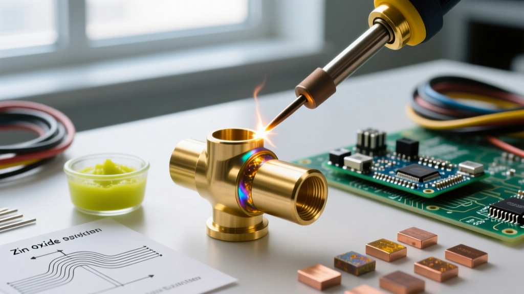
- Deoxidation: When heated past its activation temperature (typically 150°C to 180°C for rosin-based fluxes), the active compounds—such as abietic acid in natural rosin—chemically strip copper oxide (CuO) from the pad and component lead, exposing raw, reactive metal.
- Surface Tension Reduction: The molten flux blankets the joint, preventing atmospheric oxygen from reforming oxides during the soldering process while lowering the surface tension of the molten solder alloy, allowing it to 'wet' and wick into the metallurgical grain structure of the copper.
Selecting the Right Flux for Your Application
Choosing the wrong flux can lead to catastrophic board failures, including dendrite growth (electromigration) and parasitic capacitance. Below is a decision matrix for selecting the correct chemistry.
| Flux Type | IPC Classification | Best Use Case | Product Recommendation & Cost (2026) | Cleaning Required? |
|---|---|---|---|---|
| Mildly Activated Rosin (RMA) | ROL1 | General through-hole, vintage electronics repair, heavy oxidation | Kester 186 Liquid (~$14 / 2oz) | Yes (99% IPA) |
| No-Clean Tacky Paste | ROL0 | SMD rework, BGA stenciling, drag soldering fine-pitch QFPs | Chip Quik SMD291AX (~$18 / 10cc) | Optional (Aesthetic) |
| Water-Soluble (Organic Acid) | ORH1 | Automated wave soldering, heavily oxidized RF shields | MG Chemicals 8345 (~$22 / 100ml) | Mandatory (DI Water) |
Step-by-Step Tutorial: Using Soldering Flux on PCBs
This workflow assumes you are using a temperature-controlled soldering station (e.g., Hakko FX-951 or Weller WE1010) and a high-quality chisel tip, which provides superior thermal transfer compared to conical tips when working with external flux.
Phase 1: Preparation and Pre-Tinning
Never apply liquid or paste flux directly to a cold, dirty iron tip. The sudden thermal shock can cause the flux to carbonize instantly, creating a black, crusty insulator that ruins thermal transfer.
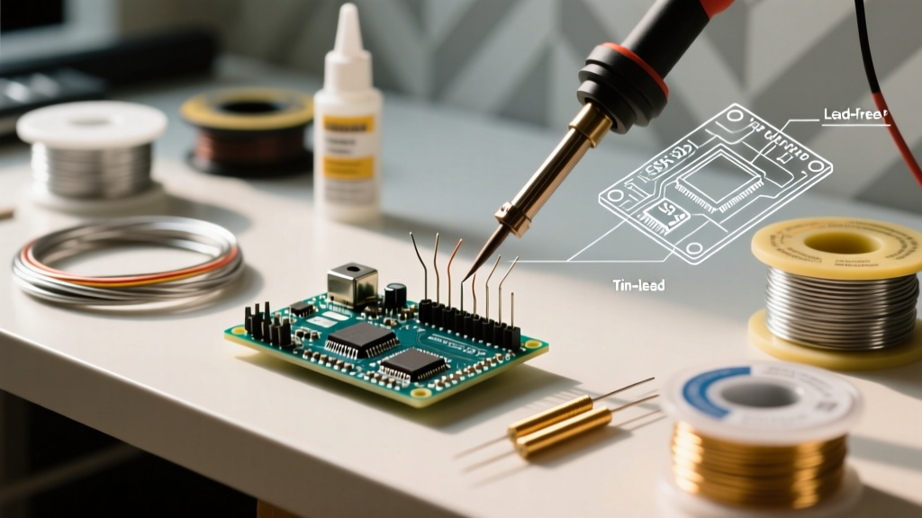
- Step 1: Set your iron to the appropriate alloy temperature. For Lead-Free SAC305 (melting point 217°C), set the station to 320°C. For Leaded 63/37 SnPb (melting point 183°C), set it to 300°C.
- Step 2: Clean the tip on a damp brass wool sponge, then apply a sacrificial coat of cored solder to 'tin' the tip. This prevents the tip's iron plating from oxidizing before it touches the PCB.
Phase 2: Precision Application Techniques
The method of application dictates the success of the joint. Over-applying flux causes messy residues and can trap flux boils under SMD components, leading to 'solder splatter'.
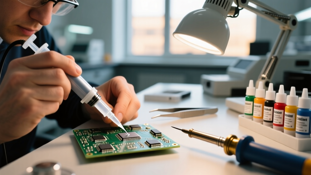
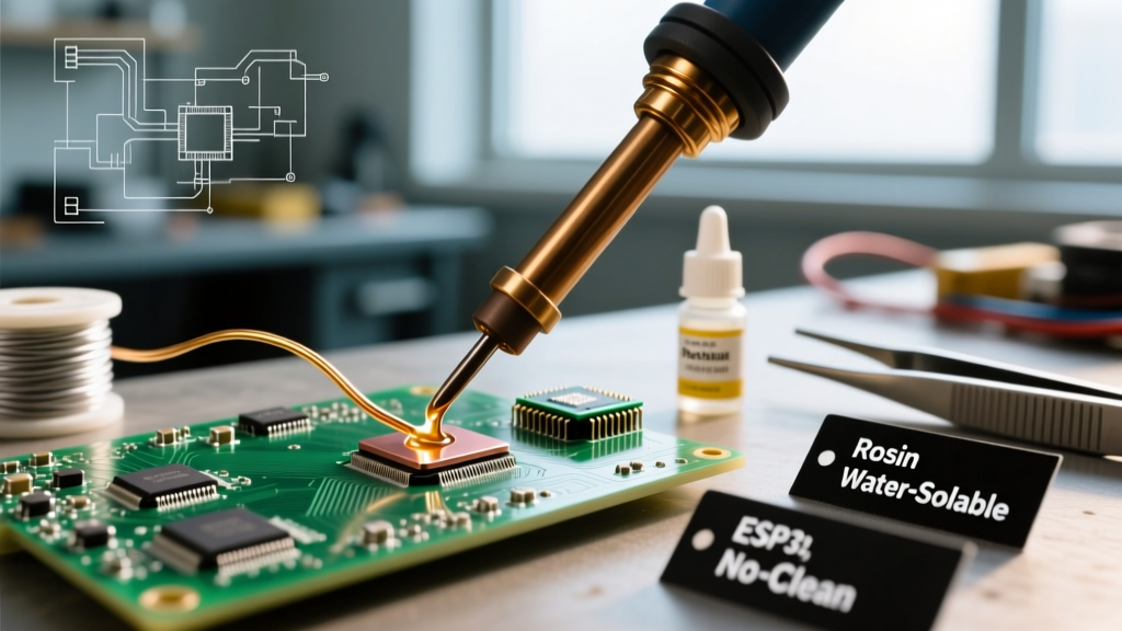
- For 0805/0603 SMD Passives: Use a tacky paste flux in a syringe with a 21-gauge blunt needle. Dispense a dot no larger than a grain of rice directly onto the pad. The tackiness will hold the component in place while you apply the iron.
- For Fine-Pitch ICs (0.5mm QFP/QFN): Apply a thin, even smear of no-clean gel flux across all pads using a clean, lint-free swab or an acid brush with the bristles trimmed to 5mm for stiffness. The flux will act as a surface tension guide, preventing solder bridges during drag soldering.
- For Heavy Ground Planes: Liquid RMA flux is superior here. Paint a generous layer over the via or ground lug. The liquid flux will penetrate the microscopic gaps in the plated through-hole (PTH), drawing the molten solder up via capillary action.
Phase 3: The Soldering Interaction (Dwell Time)
This is where most technicians fail. Flux has a strict thermal budget.
Expert Rule of Thumb: Your total iron dwell time on a single joint should not exceed 2.5 to 3.0 seconds. If the flux turns dark brown or black and stops bubbling, it has burned out. The joint will be dry and oxidized, even if it looks shiny from the solder's external flux core.
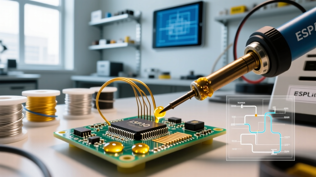
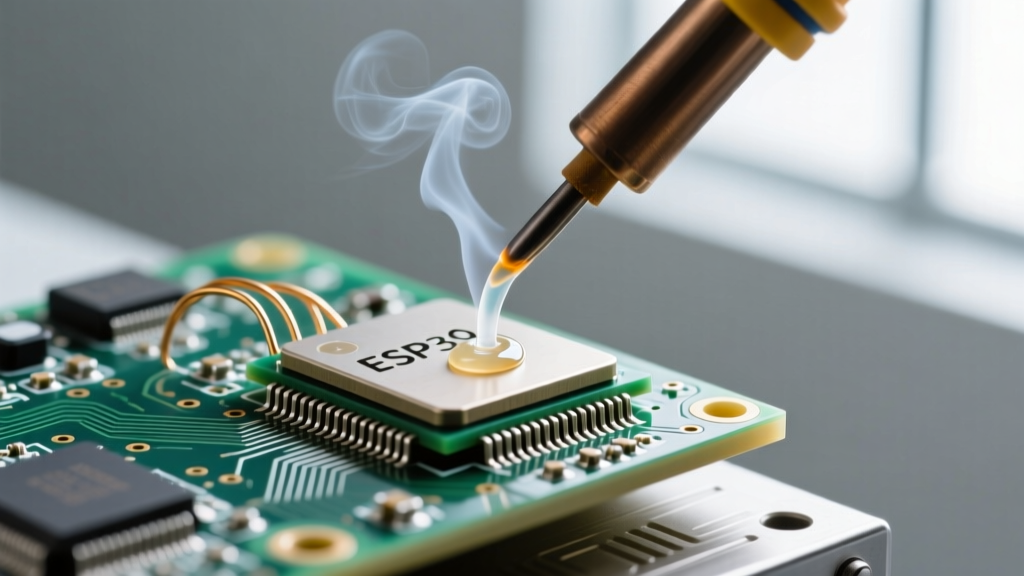
When the iron touches the fluxed pad, you should see a brief, active 'boil' as the solvents evaporate and the rosin acids activate. Introduce your solder wire to the joint, not the iron tip, within 1 second of contact. Once the solder flows into a smooth, concave fillet, remove the iron immediately.
Troubleshooting Common Flux-Related Failures
Even experienced engineers encounter anomalies when using soldering flux. Here is how to diagnose and fix them based on NASA Workmanship Standards for electronic assembly.
1. Solder Balling and Splattering
Cause: Applying too much liquid flux, or applying flux to a pad that is already too hot. The solvents in the flux flash-boil into steam, physically exploding the molten solder outward.
Solution: Apply flux to a cool board. Allow liquid flux to 'tack' (partially dry and become sticky) for 10-15 seconds before applying the iron.
2. The 'Grape' Defect (Head-in-Pillow on BGAs)
Cause: When reballing or reworking BGAs, the flux burns off before the solder paste reaches its liquidus phase, allowing the pad to re-oxidize before the solder ball collapses onto it.
Solution: Switch to a high-activity, high-thermal-mass tacky flux like Indium Corporation's NC-500, which is engineered to maintain its protective envelope up to 250°C for extended reflow profiles.
3. High-Frequency Signal Loss (Parasitic Capacitance)
Cause: Leaving standard no-clean flux residues under RF shielding or high-impedance analog nodes. While no-clean flux is non-corrosive, its dielectric constant can alter signal propagation at microwave frequencies.
Solution: For RF PCBs, always use a water-soluble flux and follow up with a rigorous deionized (DI) water cleaning process, or use a specialized low-residue solvent like MG Chemicals 4140.
Post-Soldering Cleaning Protocols
The phrase 'no-clean' is a misnomer in high-reliability environments. If your PCB will be conformal coated, subjected to high humidity, or operated in high-voltage scenarios, all flux residues must be removed to prevent electrochemical migration (dendrites).
- Manual IPA Cleaning: Use 99.9% Isopropyl Alcohol (do not use 70% rubbing alcohol, as the 30% water content will smear the rosin and drive it under components). Scrub with a stiff, natural-bristle brush, then immediately blot dry with lint-free Kimwipes before the IPA evaporates and redeposits the dissolved flux.
- Ultrasonic Agitation: For complex boards with tight BGA clearances, submerge the PCB in a heated (50°C) saponifier bath in an ultrasonic cleaner operating at 40kHz for exactly 3 to 5 minutes. Follow with a DI water rinse and a forced-air bake at 85°C for 2 hours to eliminate trapped moisture.
Final Thoughts on Modern Alloy Pairings
As the industry continues to shift toward low-temperature lead-free alloys like SN100C (Sn99.3/Cu0.7/Ni/Ge) to reduce thermal stress on multilayer ceramics, your flux chemistry must match. SN100C requires a highly active flux core to compensate for its poor wetting characteristics compared to legacy tin-lead. Always verify that your external flux's activation temperature aligns with your solder alloy's liquidus point. By treating flux as an active chemical tool rather than an afterthought, you will achieve IPC Class 3 compliant joints on every workbench project.