
The Metallurgy Behind the Melt: What Is Tinning in Soldering?
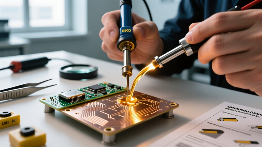
When electronics engineers, technicians, and DIY enthusiasts ask, "what is tinning in soldering?", they are often looking for a simple operational definition: the act of melting a thin layer of solder onto a component lead, wire, or soldering iron tip to prepare it for a final joint. However, from a metallurgical and reliability standpoint, tinning is the deliberate creation of an Intermetallic Compound (IMC) layer.
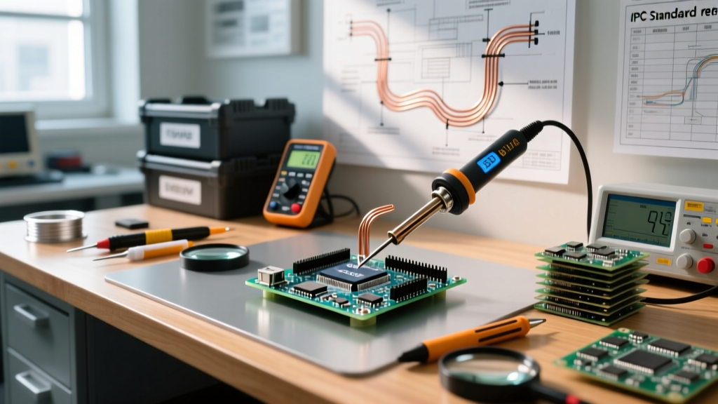
According to the IPC J-STD-001 standards, a reliable solder connection requires the molten alloy to dissolve a microscopic amount of the base metal (usually copper) and form a crystalline structure—most commonly Cu6Sn5 (copper-tin). Tinning pre-forms this IMC layer, drastically reducing the thermal time required during the final soldering phase and preventing base-metal oxidation.
"Proper tinning is not merely about coating a surface; it is about establishing a thermodynamically stable metallurgical bond that resists thermal cycling and mechanical creep." — NASA Workmanship Training Standards
Method Comparison: Manual Iron Tinning vs. Solder Pot Dip Tinning
While the fundamental chemistry remains the same, the physical method of applying the tin varies wildly depending on production volume, wire gauge, and component type. Below, we compare the two most prominent tinning methods used in prototyping and manufacturing.
Method 1: Manual Soldering Iron Tinning (Precision & Prototyping)
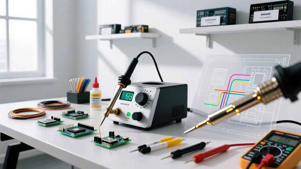
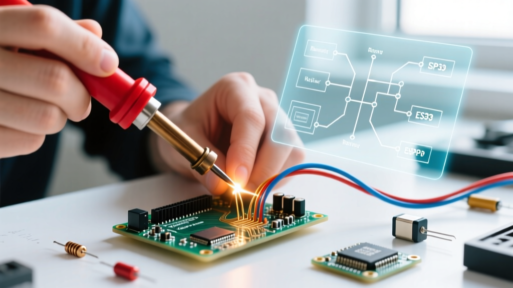
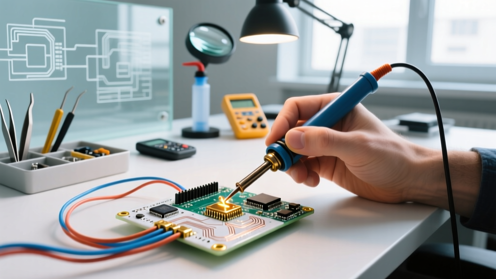
Manual tinning utilizes a temperature-controlled soldering station to apply solder and flux directly to stranded wires, PCB pads, or component leads. This method is the backbone of custom cable harness assembly and low-volume PCB rework.
- Standard Equipment: Hakko FX-888D or Weller WE1010 digital stations.
- Temperature Profiles: For traditional Sn63/Pb37 (eutectic) solder, irons are typically set to 320°C–350°C. For modern lead-free SAC305 (Sn96.5/Ag3.0/Cu0.5) alloys, temperatures must be elevated to 350°C–380°C to overcome the higher 217°C melting point and slower wetting characteristics.
- Flux Chemistry: Manual tinning relies heavily on rosin-based fluxes (ROL0 or ROL1 classifications) embedded within the solder wire core. For heavily oxidized vintage wires, an external liquid RMA (Rosin Mildly Activated) flux is applied via a brush prior to heating.
- Failure Modes: The most common error is "cold tinning," where the iron heats the solder but fails to transfer enough thermal mass to the copper wire. This results in a mechanical wrap rather than a metallurgical bond, leading to high-resistance joints that fail under current loads.
Method 2: Solder Pot / Dip Tinning (High-Volume & Heavy Gauge)
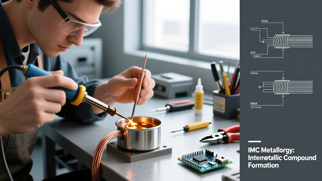
Solder pot tinning involves submerging stripped wires, lugs, or component leads directly into a crucible of molten solder. This method is vastly superior for high-volume batch processing, heavy-gauge battery cables (e.g., 4 AWG to 4/0 AWG), and magnet wire stripping.
- Standard Equipment: Hakko FX-6000 series or generic 500W–1000W static solder pots with digital PID controllers.
- The Process: Wires are first dipped in a liquid flux bath (often water-soluble ORH1 for high-activity cleaning), allowed to off-gas, and then submerged into the molten alloy for 2 to 5 seconds.
- Magnet Wire Stripping: One of the most valuable applications of a solder pot is tinning polyurethane-coated magnet wire. By setting the pot to 420°C–450°C, the molten solder instantly vaporizes the enamel insulation and tins the bare copper in a single step, eliminating the need for manual scraping or chemical stripping.
- Dross Management: A major operational cost of dip tinning is dross (tin oxide) formation. Operators must skim the surface with a perforated steel skimmer before every batch to prevent oxide inclusions in the tinned layer.
Feature Comparison Matrix: Iron vs. Dip Pot
| Feature | Manual Soldering Iron | Solder Pot / Dip Tinning |
|---|---|---|
| Initial Equipment Cost (2026) | $100 – $350 | $250 – $1,200+ |
| Throughput Speed | Low (10–30 seconds per joint) | High (2–5 seconds per batch dip) |
| Thermal Mass Capacity d> | Limited (struggles above 10 AWG) | Unlimited (handles 4/0 AWG easily) |
| Flux Requirement | Core flux usually sufficient | External liquid flux bath mandatory |
| Best Application | PCB pads, delicate ICs, custom harnesses | Heavy lugs, magnet wire, batch production |
Tinned vs. Untinned Stranded Wire: The Mechanical Reality
Why go through the effort of tinning stranded wire before inserting it into a terminal block or soldering it to a pad? The answer lies in mechanical creep and oxidation.
When untinned stranded wire is compressed under a screw terminal, the individual copper strands deform over time due to thermal expansion and contraction cycles (creep). This loosens the mechanical grip, increasing contact resistance and generating heat. Tinning binds the strands together into a single solid mass, eliminating intra-strand movement. However, as noted in the Adafruit Guide to Excellent Soldering, tinned wires should never be used in screw terminals that lack a captive washer or ferrule, as the soft solder can still deform under extreme point-load pressure from a bare screw head.
Edge Cases & Failure Modes: Dewetting vs. Non-Wetting
Understanding what is tinning in soldering also requires recognizing when the process fails. Metallurgical failures during tinning generally fall into two distinct categories:
- Non-Wetting: The molten solder contacts the base metal but fails to form an IMC layer, instead beading up like water on a waxed car. This is almost always caused by severe surface contamination (oils, heavy oxides, or incorrect flux chemistry). The solder simply cannot reach the bare copper.
- Dewetting: The solder initially wets the surface and forms an IMC layer, but then retracts into isolated islands, leaving a thin, continuous film of solder behind. Dewetting is a thermodynamic failure, often caused by prolonged exposure to high heat (which degrades the flux and oxidizes the IMC) or incompatible base metal platings (such as tinning over bare nickel without an appropriate activation flux).
Expert Troubleshooting: Reviving an Oxidized Soldering Iron Tip
The soldering iron tip itself must remain tinned to facilitate heat transfer. If a tip turns black and refuses to accept solder (a condition known as "black tip syndrome"), the iron's copper core is insulated by a thick layer of copper oxide. Do not use sandpaper or files, as this will destroy the iron plating. Follow this professional revival protocol:
- Turn the station off and let the tip cool to room temperature.
- Apply a generous dab of specialized tip tinner/cleaner (e.g., Hakko 599B or MG Chemicals Tip Tinner) to the cold tip.
- Power on the station and set it to a low temperature (250°C for leaded, 300°C for lead-free).
- As the tip heats up, the acidic compounds in the tip tinner will chemically reduce the copper oxide.
- Once the solder melts and flows, immediately wipe the tip on a damp cellulose sponge or brass wool to remove the chemical residue.
- Apply a thick layer of fresh, high-flux solder (60/40 or 63/37 is best for this, even if you normally use lead-free) to re-establish the protective IMC layer before turning the station off.
By mastering both the manual and dip methods of tinning, and understanding the underlying metallurgy, technicians can drastically reduce joint failure rates and ensure long-term reliability in both consumer electronics and high-voltage industrial applications.