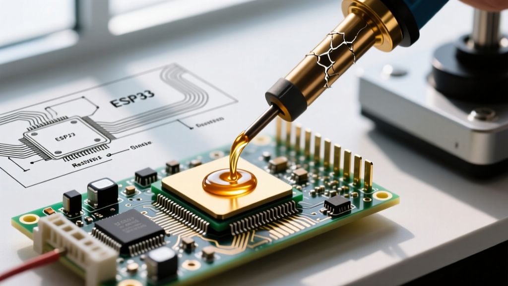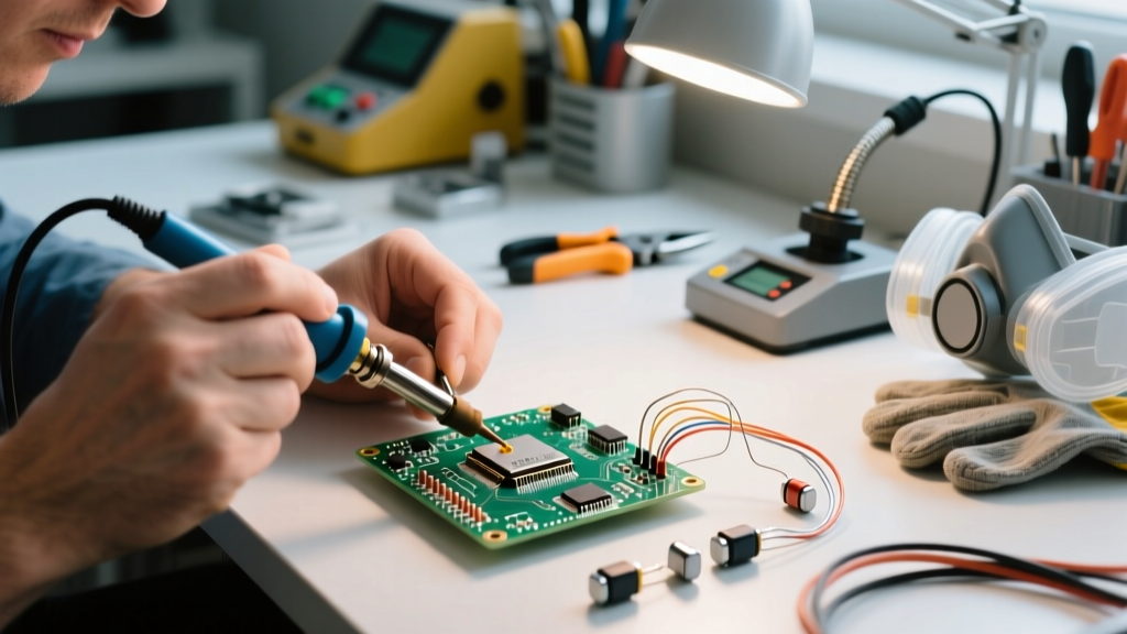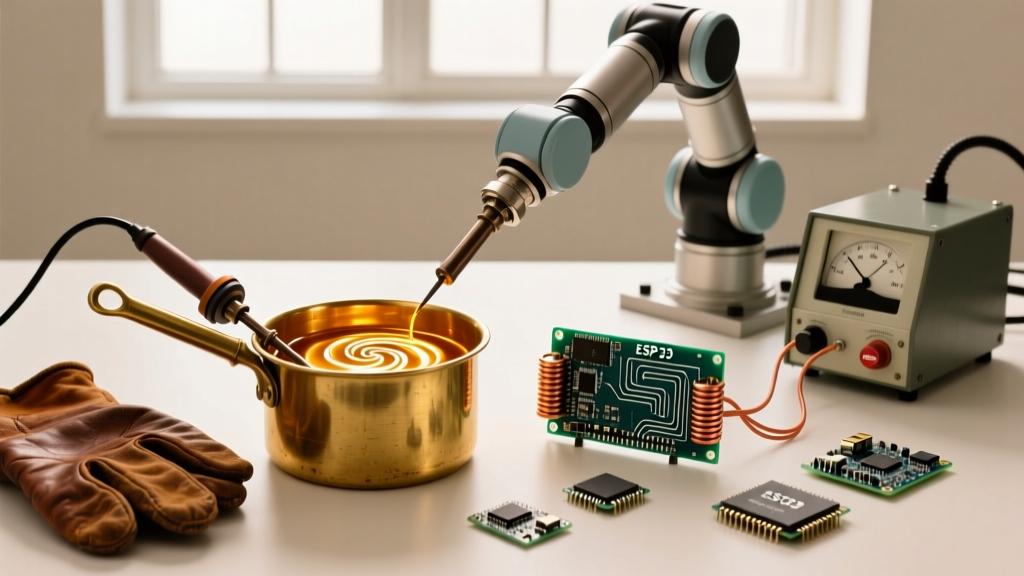

The Origins of the Soldering Dip: Early Tinning and Manual Pots
Long before the advent of printed circuit boards (PCBs) and surface-mount technology, the soldering dip was a foundational technique in metalworking, plumbing, and early electronics. In the late 19th and early 20th centuries, artisans and early radio engineers relied on manual solder pots—simple cast-iron or copper crucibles heated over open flames or early electric coils. The primary purpose of this early soldering dip was tinning: coating bare copper wires, lugs, and metal chassis components with a thin layer of molten solder to prevent oxidation and prepare surfaces for subsequent soldered joints.
During the vacuum tube era of the 1930s and 1940s, point-to-point wiring was the standard. Technicians would strip the insulation from hook-up wire, dip the bare end into a rosin flux bath, and then plunge it into a static soldering dip pot filled with molten tin-lead (Sn60/Pb40) alloy. This manual tinning process ensured that when the wire was later wrapped around a tube socket pin and heated with a soldering iron, the joint would flow instantly and reliably.
The 1950s PCB Revolution: Birth of Automated Dip Soldering
The true industrial evolution of the soldering dip occurred in the early 1950s with the mass adoption of the printed circuit board. As military and consumer electronics demanded higher component density, hand-soldering individual through-hole components became a severe manufacturing bottleneck. The industry's first attempt at automation was the static dip soldering process.
In this method, a fully populated PCB was mounted on a fixture, coated in liquid flux, and physically lowered into a large, static bath of molten solder. While revolutionary for its time, the static soldering dip presented severe engineering challenges:
- Thermal Shock: Submerging a room-temperature PCB directly into a 250°C bath caused severe warping and delamination of early phenolic substrates.
- Solder Bridging: Without the kinetic energy of a flowing wave to break surface tension, molten solder frequently bridged between closely spaced component leads.
- Icicle Formation: As the board was withdrawn from the static bath, poor drainage resulted in massive solder icicles and webbing.
According to historical archives from the Surface Mount Technology Association (SMTA), these limitations directly catalyzed the invention of wave soldering by Fry's Metals in the UK in 1956, which introduced a pump to create a dynamic, flowing wave of solder that solved the bridging and drainage issues inherent to the static dip.
The Transition to Selective and Ultrasonic Dipping
While wave soldering dominated PCB assembly for decades, the soldering dip never disappeared. Instead, it evolved into highly specialized niches. By the 1980s, the selective soldering dip emerged for mixed-technology boards where sensitive components could not withstand the thermal mass of a full wave. Today, in 2026, we also see the rise of ultrasonic solder dipping, which utilizes high-frequency acoustic cavitation to disrupt oxide layers, allowing engineers to dip-solder previously "unsolderable" materials like glass, ceramics, and aluminum without the use of chemical fluxes.
Metallurgical Challenges: Copper Dissolution and Gold Embrittlement
Operating a modern soldering dip pot requires a deep understanding of metallurgy, particularly regarding how molten alloys interact with base metals over time. The IPC (Association Connecting Electronics Industries) outlines strict parameters for bath contamination in standards like IPC-J-STD-001, primarily due to two phenomena:
Copper Leaching: In a static soldering dip pot, copper from component leads continuously dissolves into the tin matrix. At 260°C, lead-free SAC305 solder dissolves copper at a rate of approximately 2.5 microns per second. If left unchecked, the bath becomes saturated with Cu6Sn5 intermetallic compounds, raising the alloy's liquidus temperature and resulting in dull, grainy, and brittle tinned joints.
Furthermore, gold embrittlement remains a critical failure mode in aerospace and RF applications. When gold-plated RF connectors or component leads are dipped into a standard solder pot, the gold rapidly dissolves and forms AuSn4 intermetallics. If the gold concentration in the pot exceeds 3% by weight, the resulting tinned layer becomes highly brittle and prone to catastrophic mechanical failure under thermal cycling. To combat this, modern facilities utilize dedicated "gold-removal" solder pots or employ a dual-dip process where the first pot strips the gold and the second pot applies a clean tinning layer.
Modern Applications: Where the Soldering Dip Still Thrives
Despite the dominance of reflow and selective wave processes, the soldering dip remains irreplaceable for specific manufacturing and repair tasks in 2026.
| Application | Typical Alloy | Temperature Range | Primary Purpose |
|---|---|---|---|
| Standard Wire Tinning | SAC305 / Sn63Pb37 | 260°C - 280°C | Pre-tinning stranded wire for terminal crimping or PCB insertion. |
| Magnet Wire Stripping (PU) | Sn60Pb40 | 360°C - 390°C | Simultaneously burning off polyurethane enamel and tinning the copper. |
| Magnet Wire Stripping (PI) | Potassium Nitrate Bath | 450°C - 500°C | Stripping high-temp polyimide coatings (requires specialized salt pots, not standard solder). |
| Ultrasonic Tinning | Sn95Ag5 / Indium Alloys | 250°C - 300°C | Coating aluminum heat sinks or glass substrates without chemical flux. |
2026 Buyer's Guide: Choosing a Soldering Dip Station
If you are outfitting a modern repair lab, aerospace manufacturing cell, or DIY workspace, selecting the right soldering dip station is critical. The NASA Electronic Parts and Packaging (NEPP) Program emphasizes the need for precise thermal recovery and stable temperature profiles when tinning space-grade components. Here is a breakdown of the top-tier solder pots available today, categorized by use case and price point.
1. The Benchtop Standard: Hakko FX-300
Price Range: $250 - $300
Best For: General electronics repair, hobbyists, and standard wire tinning.
Key Specs: The Hakko FX-300 features a 100W ceramic heating element and a 50x50mm crucible. It utilizes a digital PID controller that maintains temperatures within ±5°C. A major advantage of the FX-300 is its interchangeable crucible design, allowing operators to swap pots quickly when switching between leaded and lead-free alloys, thereby preventing cross-contamination. However, its thermal recovery time struggles when dipping large-gauge wires or heavy copper ground planes.
2. The Industrial Workhorse: Pace ST 300
Price Range: $450 - $550
Best For: High-volume production tinning and heavy thermal mass components.
Key Specs: The Pace ST 300 offers a larger 100x100mm bath area and a robust 200W heater. It excels in thermal recovery, making it ideal for tinning thick RF coaxial cables or large transformer leads. The ST 300 also includes an integrated dross skimming tray and adjustable temperature profiles specifically calibrated for high-temperature lead-free alloys like SAC305 and SN100C.
3. The Precision Aerospace Choice: Metcal SP200
Price Range: $600 - $750
Best For: Military, medical, and aerospace manufacturing (IPC Class 3).
Key Specs: Metcal utilizes proprietary SmartHeat® induction technology. Instead of a thermostat that cycles on and off (causing temperature overshoot and undershoot), the SP200 uses RF induction to heat the solder crucible directly based on its magnetic permeability. When a cold wire is dipped into the bath, the alloy's temperature drops, its magnetic properties change, and the system instantly delivers more power to that exact spot. This guarantees zero thermal overshoot, protecting highly sensitive, thermally fragile component leads from damage.
Maintenance and Dross Management
Regardless of the model chosen, maintaining a soldering dip pot requires rigorous dross management. In a static pot, oxidation occurs continuously at the air-solder interface. Operating a pot at 280°C without a nitrogen blanket or liquid dross-reducing agent (like Kester 186 or similar organic acids) can generate up to 15 grams of dross per hour. Modern best practices dictate skimming the pot every two hours of active use and performing a full bath analysis via X-ray fluorescence (XRF) every 30 days to monitor copper and gold contamination levels. Neglecting this maintenance not only ruins the tinning finish but accelerates the corrosion of the crucible itself, leading to catastrophic pot failures and molten solder spills.
Conclusion
The soldering dip has journeyed from a rudimentary blacksmith's tinning crucible to a highly controlled, metallurgically complex process essential to modern electronics manufacturing. While wave and reflow technologies conquered the PCB assembly floor, the soldering dip remains the undisputed champion of component preparation, wire tinning, and specialized material joining. Understanding its history, respecting its metallurgical boundaries, and investing in precision temperature-controlled equipment ensures that this oldest of soldering methods continues to deliver flawless results in the most demanding 2026 applications.