
The ITAD Bottleneck: Why Facilities Need to Upgrade Soldered RAM
As of 2026, the enterprise laptop and ultrabook market has almost entirely transitioned to Low Power Double Data Rate (LPDDR) memory architectures. Driven by the demand for thinner chassis, longer battery life, and the unified memory requirements of ARM-based silicon, manufacturers have abandoned socketed SO-DIMM slots in favor of directly soldering RAM chips to the motherboard. For the IT Asset Disposition (ITAD) and professional repair industry, this shift has created a massive bottleneck. Devices equipped with 8GB of soldered RAM are increasingly being classified as e-waste or liquidated at severe discounts because modern enterprise workflows demand a minimum of 16GB or 32GB.
This begs a critical question for high-volume repair facilities and micro-soldering specialists: can you actually upgrade soldered RAM at an industry scale? The short answer is yes, but it requires advanced Ball Grid Array (BGA) rework capabilities, a deep understanding of memory controller training, and strict thermal profiling. This guide explores the technical realities, equipment requirements, and economic viability of performing LPDDR BGA upgrades in a professional ITAD environment.
The Physics and Architecture of LPDDR5X BGA Rework
Upgrading soldered RAM is fundamentally different from replacing a discrete CPU or GPU. Memory chips are often placed in dense clusters, sharing tight trace routing and decoupling capacitors. The transition from LPDDR4X to LPDDR5 and the current LPDDR5X standard has drastically reduced the BGA pitch. While older LPDDR3 chips utilized a relatively forgiving 0.8mm or 0.65mm pitch, modern LPDDR5X chips frequently utilize a 0.5mm or even 0.4mm pitch.
According to the JEDEC JESD209-5 standard for LPDDR5 memory, the physical footprint and ball map are highly optimized for signal integrity at speeds exceeding 6400 MT/s. This means that when a technician attempts to upgrade soldered RAM, the margin for error regarding solder bridge formation and pad alignment is measured in microns. Furthermore, the substrate thickness of modern ultrabook motherboards (often 0.8mm or less) makes them highly susceptible to thermal warping during the reflow process, which can lead to catastrophic pad cratering if not properly supported.
Professional Equipment Arsenal for Memory Upgrades
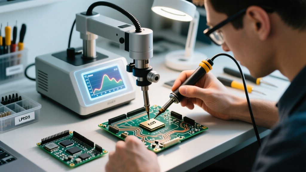
You cannot perform reliable, high-yield BGA memory upgrades with a standard hot air rework station. ITAD facilities investing in this service line must procure specialized equipment to ensure repeatable thermal profiles and precise optical alignment.
- BGA Rework Stations: High-end optical alignment systems like the Finetech Fineplacer lambda or Jovy Systems JV-5300 are mandatory. These machines utilize closed-loop thermocouple feedback and split-vision optics to align 0.4mm pitch BGA spheres to motherboard pads. Equipment costs range from $15,000 to over $60,000 depending on automation levels.
- Pre-Heating Matrices: Infrared or hot-air bottom pre-heaters (such as those integrated into the Quick 861DW ecosystem or standalone Hakko FR-830 units) are required to bring the entire motherboard to a baseline temperature of 130°C to 150°C. This prevents thermal shock and reduces the delta-T required from the top heat nozzle.
- Stencil and Reballing Gear: Direct-print stainless steel stencils (0.12mm thickness) paired with precision squeegees are used for applying solder paste. For harvested donor chips, automated reballing fixtures using SAC305 (lead-free) or Sn63Pb37 (tin-lead) solder spheres are necessary.
- Flux and Chemistry: High-tack, no-clean fluxes like Amtech NC-559-V2-TF or Kingbo RMA-223 are essential to prevent oxidation during the prolonged heat exposure required for multi-chip memory banks.
Step-by-Step Industry Workflow: The BGA Rework Process
Executing a successful RAM upgrade requires a disciplined, step-by-step approach that adheres to the IPC-7095 BGA design and assembly guidelines. Below is the standard operating procedure utilized by tier-one micro-soldering labs.
1. Teardown, Masking, and Support
The motherboard is stripped of all heat sinks, CMOS batteries, and delicate ribbon cables. High-temperature Kapton tape and aluminum foil are used to mask adjacent components, particularly microscopic 0201 decoupling capacitors located millimeters from the RAM BGA pads. The board is then secured to a custom-machined aluminum support plate to prevent PCB sagging during the liquidus phase.
2. Thermal Profiling and Desoldering
A ramp-soak-spike thermal profile is programmed into the BGA station. The bottom pre-heater brings the board to 150°C over 90 seconds. The top nozzle applies a controlled flow of nitrogen-assisted hot air, ramping to 235°C (for lead-free SAC305 solder). Once the solder reaches the liquidus state, the machine's vacuum pickup head gently lifts the original 8GB LPDDR5 chip. Critical Rule: Never apply mechanical prying force. If the chip does not lift freely, the solder has not fully liquefied, and prying will rip the copper pads from the fiberglass substrate.
3. Pad Dressing and Site Preparation
The exposed BGA pads are cleaned using Chemtronics desoldering braid (2.5mm width) and copious amounts of isopropyl alcohol (99%+ purity). The goal is to achieve perfectly flat, uniform pads with zero residual solder doming, which is crucial for the 0.4mm pitch of LPDDR5X chips.
4. Paste Printing and Chip Placement
Using a direct-print stencil, a precise volume of Type 4 or Type 5 solder paste is applied to the motherboard pads. The new 16GB LPDDR5X IC is picked up via the BGA station's vacuum nozzle, aligned using the split-beam optical camera system, and placed onto the paste with a programmed Z-axis force of roughly 100 grams to ensure pad contact without squeezing out excess paste.
5. Reflow and Controlled Cooling
The board undergoes the final reflow spike, holding above liquidus (TAL) for exactly 45 to 60 seconds to allow for proper intermetallic compound (IMC) formation. The cooling phase is actively managed with forced ambient air to prevent the formation of brittle grain structures in the solder joints.
ITAD Cost-Benefit Matrix: Motherboard Swap vs. BGA Upgrade
For ITAD managers, the decision to upgrade soldered RAM must make financial sense. Below is a comparative analysis of replacing a proprietary motherboard versus performing a BGA memory upgrade on a typical 2025 enterprise ultrabook.
| Metric | Motherboard Replacement (OEM) | BGA RAM Upgrade (In-House Rework) |
|---|---|---|
| Component Cost | $450 - $850 (OEM proprietary board) | $25 - $45 (LPDDR5X 16GB IC) |
| Labor Time | 30 - 45 minutes (Teardown/Swap) | 90 - 120 minutes (Rework & QA) |
| Equipment Amortization | N/A (Standard hand tools) | $8.50 per board (Based on $50k station over 6k units) |
| E-Waste Impact | High (Discarding functional CPU/Board) | Minimal (Only original RAM ICs scrapped) |
| Yield / Success Rate | 99.9% (Assuming OEM part availability) | 92% - 96% (Dependent on technician skill) |
Industry Insight: While the upfront labor and equipment costs for BGA rework are higher, the elimination of OEM motherboard supply chain dependencies and the drastic reduction in e-waste make RAM upgrading highly profitable for ITAD facilities processing over 5,000 units annually.
Edge Cases, BIOS Whitelists, and Failure Modes
Successfully soldering the chip to the board is only half the battle. The most complex hurdle when attempting to upgrade soldered RAM is the firmware and memory training architecture.
The Memory Reference Code (MRC) Hurdle
Unlike SO-DIMM modules, which contain an SPD (Serial Presence Detect) EEPROM that tells the motherboard the exact capacity, speed, and timings of the installed RAM, soldered LPDDR chips do not have a separate SPD chip. The motherboard BIOS relies on hardcoded Memory Reference Code (MRC) or reads mode registers directly from the LPDDR IC. If an OEM has locked the BIOS to only accept an 8GB configuration, installing a 16GB chip will result in a POST failure, typically indicated by a repeating memory error LED code or an infinite boot loop. Advanced repair shops must utilize hardware programmers (like the SVOD4 or RT809H) to read, modify, and flash the BIOS/ME region to unlock higher memory density support before the board will POST.
Common Failure Modes in LPDDR Rework
- Pad Cratering: Occurs when the PCB is subjected to mechanical flexing while the solder is in a semi-solid state during cooling. This breaks the via barrel connections beneath the BGA pad, resulting in intermittent memory channel failures that are nearly impossible to diagnose without X-ray inspection.
- Solder Bridging: Highly prevalent on 0.4mm pitch LPDDR5X chips. Caused by using Type 3 solder paste (particles are too large for the micro-apertures) or applying excessive Z-axis placement force, squeezing paste between adjacent pads.
- Thermal Degradation of the IC: LPDDR chips are sensitive to prolonged heat. If the time above liquidus (TAL) exceeds 90 seconds, the internal silicon die can delaminate from the chip's organic substrate, resulting in a completely dead memory IC despite perfect solder joints.
Conclusion: The Future of Soldered Memory in ITAD
The ability to upgrade soldered RAM represents the cutting edge of the micro-soldering and ITAD industries. As OEMs continue to push toward unified, soldered architectures to maximize battery space and minimize chassis thickness, the volume of artificially bottlenecked 8GB devices will only increase. By investing in precision BGA rework stations, mastering advanced thermal profiles, and understanding the intricacies of BIOS memory training, professional repair facilities can reclaim thousands of dollars in otherwise depreciated enterprise assets, turning a proprietary design limitation into a highly profitable service vertical.