
The Hidden Trap: Understanding Gold Embrittlement
When hobbyists and professionals transition from standard HASL (Hot Air Solder Leveling) boards to gold-finished PCBs, they often assume the soldering process remains identical. This assumption leads to catastrophic joint failures. The primary enemy when soldering gold is a metallurgical phenomenon known as gold embrittlement.
According to research from the NASA Electronic Parts and Packaging (NEPP) Program, when gold dissolves into a molten tin-based solder alloy, it forms a gold-tin intermetallic compound (IMC), specifically AuSn4. If the gold concentration in the solder joint exceeds 3% to 5% by weight, the joint becomes highly brittle and will fracture under minimal mechanical or thermal stress. Understanding the type of gold finish on your board or wire is the first step in troubleshooting and preventing these failures.
ENIG vs. Electroplated Hard Gold
Not all gold finishes are created equal. In modern PCB manufacturing, you will primarily encounter two types:
- ENIG (Electroless Nickel Immersion Gold): The gold layer is ultra-thin (0.05µm to 0.1µm) and serves only to protect the underlying nickel from oxidation. As of 2026, ENIG adds roughly $15 to $45 per batch compared to HASL at major fabs. It is generally safe to solder directly to ENIG because the gold volume is negligible.
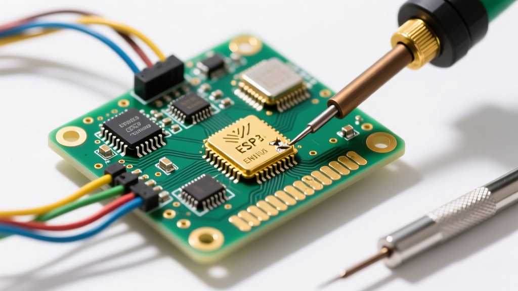
- Electroplated Hard Gold: Used for edge connectors (like PCIe slots) and high-wear contacts. This layer is thick (1µm to 3µm+) and contains cobalt or nickel hardeners. Soldering directly to hard gold without stripping will almost certainly cause embrittlement.
Troubleshooting Matrix: Common Gold Soldering Defects
When soldering gold-plated surfaces, visual inspection is your first line of defense. The IPC J-STD-001 standard outlines strict criteria for solder wetting and joint integrity. Below is a diagnostic matrix for common failures encountered on gold surfaces.
| Visual Defect | Root Cause | Corrective Action |
|---|---|---|
| Dull, grainy, or fractured joint on ENIG | Nickel oxidation (Black Pad Syndrome) or insufficient flux activity breaking through the immersion gold. | Switch to a high-activity ROL0/ROL1 flux (e.g., Kester 186); verify PCB storage humidity limits. |
| Joint cracks upon cooling or minimal bending | Gold embrittlement (AuSn4 formation) caused by soldering directly to thick hard-gold plating. | Strip the gold via a tinning pool or solder bath before executing the final structural solder joint. |
| Solder balls up, refuses to wet the pad | Organic contamination, fingerprint oils, or a passivation layer on the gold surface. | Clean aggressively with 99% IPA and apply a tack flux like Amtech NC-559-V2-TF before heating. |
| Solder wicks up the wire, leaving a dry pad | Excessive heat applied to the wire rather than the pad, or improper flux distribution. | Pre-tin the pad first. Apply iron tip to the pad, feed solder to the joint, then introduce the wire. |
FAQ: Preparation, Stripping, and Wire Soldering
Do I need to strip the gold off ENIG pads before soldering?
No. The gold layer on ENIG is so thin that it dissolves instantly into the molten solder, leaving you with a reliable tin-nickel IMC. The gold volume is far below the 3% embrittlement threshold. Attempting to mechanically strip or pre-tin ENIG pads unnecessarily risks damaging the delicate nickel layer underneath, leading to non-wettable pads.
What about soldering wires to gold-plated terminals or thick hard gold?
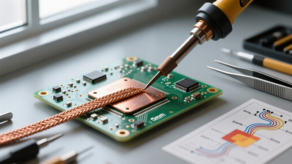
This requires a different approach. If you are soldering to gold-plated banana plugs, thick gold wires, or hard-gold edge connectors, you must manage the gold dissolution. The industry-standard method is tinning and wiping. You apply a large blob of fresh solder to the gold surface, let the gold dissolve into the blob, and then use copper solder wick (like Desoldering Braid from Chemtronics) to remove that gold-contaminated solder. You then apply a second blob of fresh solder to the now-exposed base metal (usually copper or nickel) and proceed with your wire soldering.
Why does my solder joint on ENIG look slightly darker than HASL joints?
This is normal. The underlying metal in ENIG is nickel, not copper. The resulting IMC is primarily Ni3Sn4 rather than Cu6Sn5. Nickel-tin intermetallics naturally exhibit a slightly duller, darker, or more matte finish compared to the bright shine of copper-tin joints. Do not mistake this for a cold joint, provided the solder has properly wetted the edges and formed a smooth fillet.
Step-by-Step: Soldering Gold-Plated Wires to PCBs
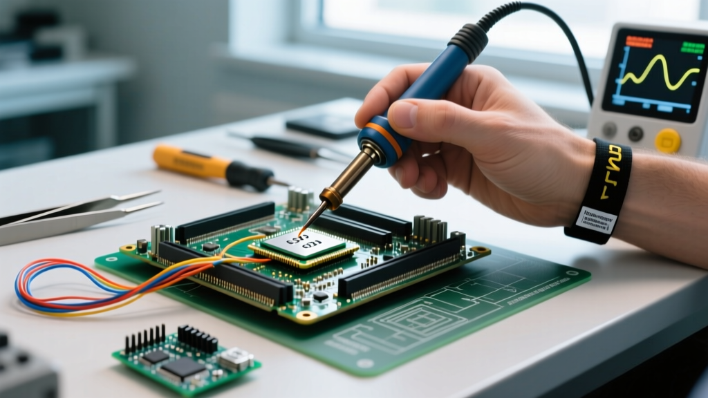
When attaching gold-plated wires (such as high-end audio cables or aerospace-grade PTFE wires) to standard PCB pads, follow this precise sequence to ensure mechanical and electrical integrity:
- Mechanical Preparation: Strip the PTFE or silicone insulation. If the wire is stranded, twist it tightly. Do not tin the wire yet.
- Flux the Pad: Apply a no-clean or RMA liquid flux to the PCB pad. For 2026 DIY standards, Chip Quik SMD291AX10 in a syringe offers excellent tack and activation.
- Pre-Tin the Pad: Set your station (e.g., Hakko FX-951 or Weller WE1010) to 340°C for Sn63Pb37 or 360°C for SAC305 lead-free. Touch the iron to the pad and feed just enough solder to create a convex dome.
- Flux the Wire: Dip the bare gold-plated wire into liquid flux.
- Pre-Tin the Wire: Briefly touch the iron to the wire to melt a thin coat of solder over the gold strands. Time this to under 2 seconds to prevent the gold from fully dissolving and weakening the wire strands.
- The Final Marriage: Place the pre-tinned wire onto the pre-tinned pad. Apply the iron to the side of the wire/pad junction. The two solder masses will fuse instantly. Remove the iron and hold the wire perfectly still for 3-5 seconds until the solder transitions from liquid to solid.
Flux Selection and Temperature Profiles
Gold is a noble metal and does not oxidize in air, which tricks many into thinking flux is unnecessary. However, the base metal beneath the gold (or the nickel in ENIG) can suffer from micro-oxidation, and surface contaminants will ruin wetting.
Expert Tip: Never use highly acidic plumbing fluxes or aggressive water-soluble fluxes on gold-plated electronics. The halides can become trapped under components and cause galvanic corrosion between the gold and the underlying metals. Stick to ROL0 (Rosin Low Activity) or REL0 (Rosin Equivalent Low Activity) classifications.
Recommended Temperature Profiles
- Leaded Solder (Sn63Pb37 / Sn60Pb40): Tip temperature 330°C – 350°C. Dwell time: 2 to 3 seconds per joint.
- Lead-Free Solder (SAC305): Tip temperature 360°C – 380°C. Dwell time: 3 to 4 seconds. Use a chisel tip rather than a conical tip to maximize thermal transfer, as lead-free alloys have a higher liquidus point (217°C+).
Final Thoughts on Gold Metallurgy
Soldering gold requires a shift in mindset from visual aesthetics to metallurgical reality. A shiny gold pad is merely a protective shield; your actual solder joint is forming with the metal hiding underneath. By respecting the 3% embrittlement threshold, utilizing the correct tinning and stripping techniques for hard gold, and trusting the ultra-thin nature of ENIG, you will achieve joints that meet the rigorous reliability standards outlined by the Surface Mount Technology Association (SMTA). Always prioritize proper flux activation and precise thermal management over brute-force heating.