
The Core Prototyping Dilemma: Speed vs. Signal Integrity
When transitioning a circuit from a solderless breadboard to a permanent state, engineers and hobbyists face a critical decision. The method you choose for prototype board soldering dictates not only the mechanical reliability of your device but also its high-frequency performance, power distribution efficiency, and overall build time. While custom printed circuit boards (PCBs) are cheaper than ever in 2026, the immediate feedback loop of manual prototyping remains indispensable for analog tweaking, quick repairs, and proof-of-concept validation.
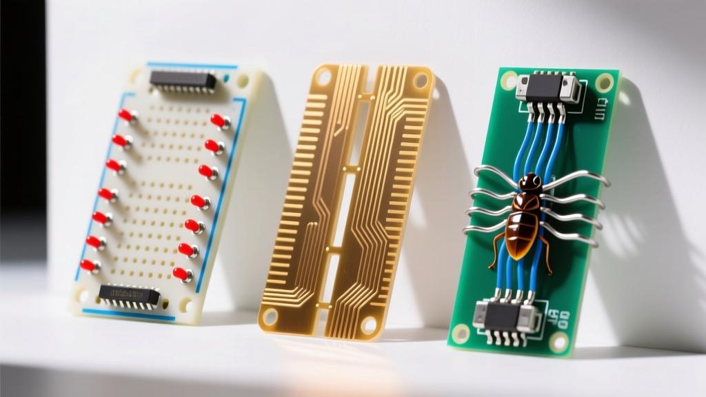
This guide provides a deep-dive comparison of the three dominant manual prototyping methods: Pad-per-hole perfboard, copper stripboard (Veroboard), and dead-bug enamel wire routing. We will evaluate them based on real-world material costs, parasitic electrical characteristics, and specific failure modes.
Method 1: Pad-Per-Hole Perfboard (The Discrete Approach)
Pad-per-hole perfboard consists of an FR4 or phenolic substrate with a 0.1-inch (2.54mm) grid of plated or unplated copper pads. Each pad is electrically isolated from its neighbors, requiring the builder to use component leads or jumper wires to create connections.
Material Specs and Pricing
- FR4 Fiberglass (Plated Through-Hole): The premium choice. Pads are wrapped through the board, meaning heat and mechanical stress are distributed across both sides. A standard 3x7 inch board costs between $3.50 and $5.00.
- Phenolic Paper (Non-Plated): The budget option. Pads are merely glued to the surface. A 3x7 inch board costs around $1.50. However, phenolic boards are highly susceptible to pad lifting if your iron dwells for more than 3-4 seconds per joint.
Perfboard excels in low-frequency analog circuits, audio amplifiers, and discrete transistor logic where point-to-point wiring minimizes stray capacitance between adjacent nodes. According to SparkFun's through-hole soldering guide, maintaining a clean iron tip and using adequate flux is critical when bridging non-adjacent pads on perfboard to avoid cold joints.
Method 2: Stripboard / Veroboard (The Continuous Trace)
Stripboard features continuous copper strips running along one axis of the 0.1-inch grid. This method drastically reduces the need for jumper wires, as power rails and ground buses are inherently built into the board's topology.
The Art of Track Cutting
To use stripboard effectively, you must break the continuous copper tracks to isolate specific IC pins or prevent short circuits. This is done using a dedicated track cutter (a specialized end-mill tool costing roughly $8) or a 3mm drill bit twisted by hand. Edge Case Warning: Incomplete track cuts are the number one cause of debugging nightmares on stripboard. Always verify isolation with a multimeter's continuity beep test before soldering sensitive microcontrollers.
Stripboard is the superior choice for digital logic, microcontroller breakouts, and power distribution networks. However, the parallel copper strips introduce a parasitic capacitance of approximately 2pF to 5pF per inch between adjacent tracks. This makes stripboard highly unsuitable for RF circuits or high-speed digital buses (like SPI running above 10MHz), where this capacitance will round off signal edges and cause data corruption.
Method 3: Dead-Bug and Enamel Wire Routing (The RF Choice)
When signal integrity is paramount, and standard prototype board soldering methods introduce too much parasitic inductance or capacitance, engineers turn to the 'dead-bug' method. This involves gluing ICs upside down (legs in the air) to a blank, unetched copper-clad FR4 board using cyanoacrylate (super glue). The solid copper surface acts as a continuous, ultra-low-impedance ground plane.
Connections are made using 30 AWG or 28 AWG polyurethane-enameled copper wire (often called magnet wire). The polyurethane insulation melts instantly upon contact with a 350°C soldering iron tip, eliminating the need to strip wires. This method is heavily favored in RF design, high-speed op-amp testing, and ultra-compact sensor nodes where commercial prototyping boards fall short.
Head-to-Head Comparison Matrix
| Feature | Pad-Per-Hole (FR4) | Stripboard (Veroboard) | Dead-Bug (Blank Copper) |
|---|---|---|---|
| Build Time | Moderate (High wire routing) | Fast (Built-in traces) | Slow (Requires precision) |
| Signal Integrity | Good (Low capacitance) | Poor (High track capacitance) | Excellent (Solid ground plane) |
| Mechanical Strength | High | High | Moderate (Glue degradation) |
| Cost (per 3x7 inch) | $3.50 - $5.00 | $3.00 - $4.50 | $2.00 (Blank FR4 + Glue) |
| Best Application | Analog, Audio, General DIY | Digital Logic, Power Rails | RF, High-Speed, Op-Amps |
Critical Material Selection for Prototype Board Soldering
The success of your prototype relies heavily on your consumables. The Adafruit Guide to Excellent Soldering emphasizes that flux chemistry is just as important as the solder alloy itself.
Solder Alloy and Diameter
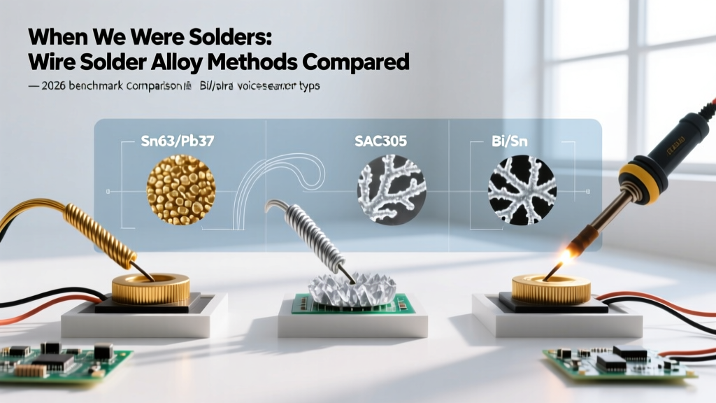
For manual prototype board soldering, 63/37 Tin-Lead (Sn63Pb37) remains the gold standard due to its eutectic properties—it transitions from liquid to solid instantly, preventing micro-fractures caused by component movement during cooling. A diameter of 0.031 inches (0.8mm) is optimal for 0.1-inch pitch through-hole work. If you are mandated to use lead-free solder, opt for SAC305 (Sn96.5/Ag3.0/Cu0.5) with a rosin-based flux core, and increase your iron tip temperature from 320°C to 360°C to compensate for the higher melting point.
Flux Supplementation
Even with flux-cored wire, manual prototyping often requires additional flux to ensure proper wetting, especially when bridging pads with jumper wires. Use a No-Clean liquid flux pen (like Amtech or MG Chemicals 8341) for general work. If you are adapting SMD breakout boards onto through-hole perfboard, a tacky rosin flux (like Chip Quik SMD291AX) applied with a syringe will prevent the solder wicking away from the fine-pitch pads.
Common Failure Modes and Edge Cases
Understanding how prototype boards fail allows you to design around their physical limitations.
- Ground Bounce on Perfboard: Because perfboard lacks a ground plane, long jumper wires used for ground returns act as inductors. In circuits with switching regulators or high-current MOSFETs, this inductance causes voltage spikes (ground bounce). Solution: Use 20 AWG bare copper wire laid flat across the back of the board, soldered at every available pad, to create a pseudo-ground plane.
- Flux Residue Conductivity on Stripboard: Water-soluble fluxes are highly corrosive and conductive if not cleaned. On stripboard, where tracks are separated by only 1.5mm of exposed FR4, residual flux can create high-impedance leakage paths that ruin high-gain analog sensor readings. Solution: Always use No-Clean or Rosin (RMA) flux for stripboard, or wash thoroughly with 99% isopropyl alcohol and a hog-bristle brush.
- Thermal Pad Delamination: When soldering large ground pins (like the thermal pad on a TO-220 voltage regulator) to a perfboard, the massive copper area acts as a heatsink, drawing heat away from the joint. This leads to extended dwell times and pad delamination. Solution: Pre-heat the board with a hot air rework station at 120°C before applying the soldering iron.
When to Abandon Prototype Boards for Custom PCBs
While mastering prototype board soldering is a fundamental engineering skill, knowing when to stop is equally important. You should transition to a manufactured custom PCB (via services like JLCPCB or PCBWay, which offer 5 boards for roughly $2 plus shipping in 2026) when your project meets any of the following criteria:
- Component Count Exceeds 40: The cognitive load of routing wires manually increases the risk of wiring errors exponentially past this threshold.
- Signal Frequencies Exceed 20MHz: The uncontrolled impedance and lack of proper return paths on manual boards will cause severe EMI and signal degradation.
- Current Exceeds 3 Amps: Standard 22 AWG jumper wires and 1oz perfboard traces will overheat. Manufactured PCBs allow you to specify 2oz copper and route 50-mil wide traces for high-current paths.
For everything else, selecting the right prototyping method and applying meticulous soldering technique—as outlined in professional rework standards like the IPC-7711/7721 guidelines—will yield a robust, test-ready prototype that can survive the rigors of the lab bench.