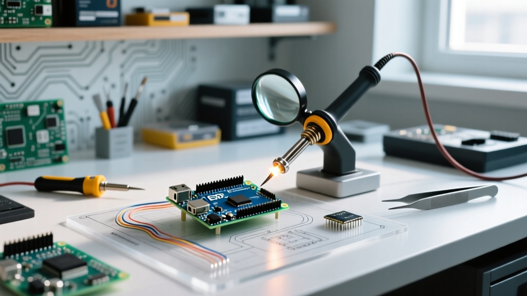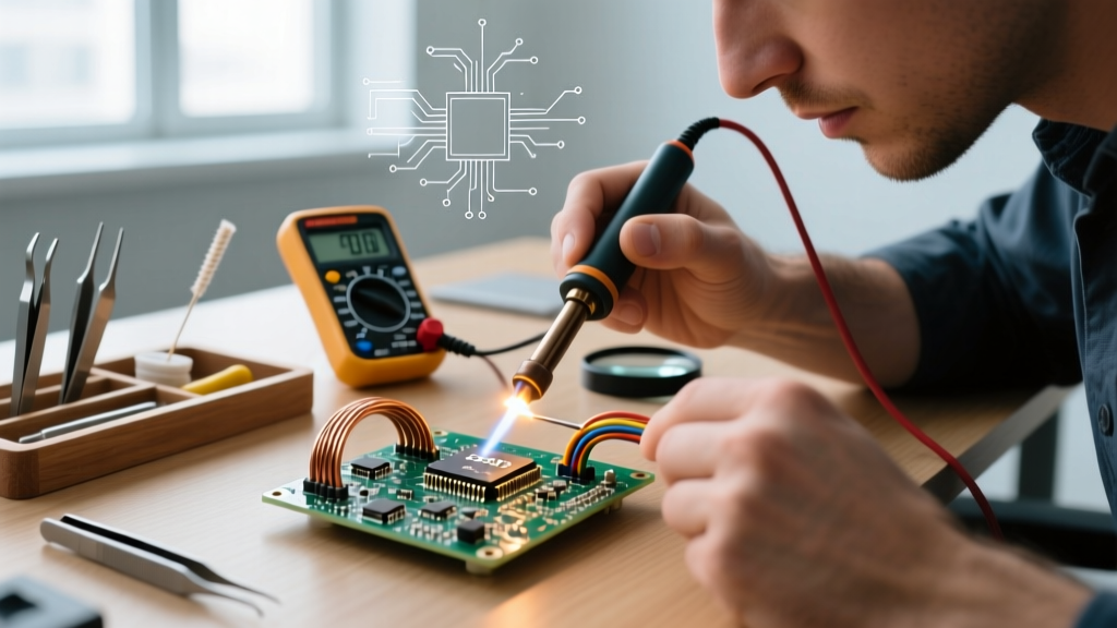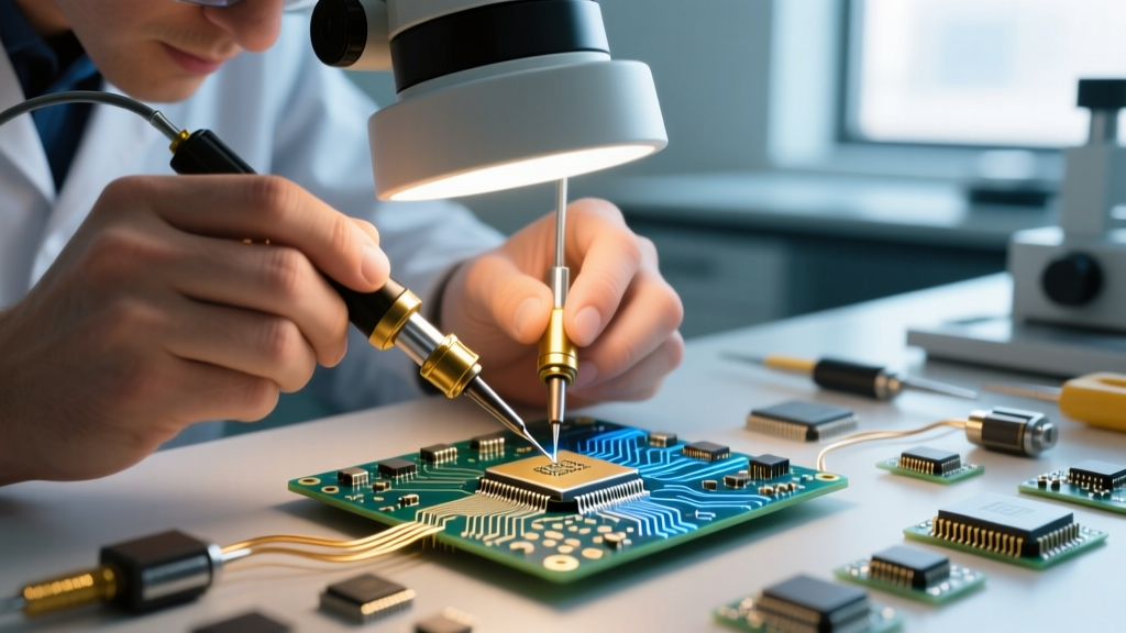

The Hidden Liability of Stock Image Soldering in Electronics Marketing
In the rapidly expanding DIY electronics and microcontroller market of 2026, visual documentation is just as critical as the bill of materials. Whether you are launching a new Raspberry Pi HAT, selling a through-hole DIY clock kit on Amazon, or writing an educational blog on surface-mount device (SMD) rework, the imagery you use dictates user success. However, a pervasive and technically dangerous trend has infected the industry: stock image soldering.
Stock image soldering refers to the practice of using generic, commercially licensed photographs of people soldering to illustrate technical guides, product listings, or marketing materials. While cost-effective upfront, these images are almost universally populated with severe technical inaccuracies that violate established IPC Standards and NASA Workmanship Standards. For buyers, educators, and kit manufacturers, relying on these visuals is not just an aesthetic failure—it is a functional liability that leads to cold joints, damaged PCBs, and high return rates.
Method Comparison: Generic Stock Visuals vs. IPC-Compliant Reality
To understand the gap between stock image soldering and actual best practices, we must compare the visual tropes found in generic media against the strict requirements of IPC-A-610 (Acceptability of Electronic Assemblies). The following matrix breaks down the most common discrepancies.
| Visual Element | Stock Image Soldering Trope | IPC-A-610 / Real-World Standard | Impact on Learner |
|---|---|---|---|
| Iron Grip | "Dagger grip" (fist wrapped around handle) | "Pencil grip" for precise 45-degree approach | Promotes poor pad access and thermal runaway |
| Tip Geometry | Needle-like conical tips | Chisel, bevel, or hoof tips for maximum surface contact | Results in insufficient heat transfer and cold joints |
| Solder Feed | Feeding solder directly to the iron tip | Feeding solder to the pad/lead junction | Teaches "painting" with solder, causing dry joints |
| Joint Profile | Large, spherical beads sitting on the pad | Concave fillets with smooth wetting edges | Normalizes non-wetting and insufficient solder volume |
4 Fatal Technical Errors in Stock Soldering Photography
When evaluating visual assets for a soldering buyer guide or kit manual, it is crucial to audit the imagery for specific failure modes. Here are the four most common technical violations found in stock image soldering, and why they ruin the learning experience.
1. The Dagger Grip and Loss of Fine Motor Control
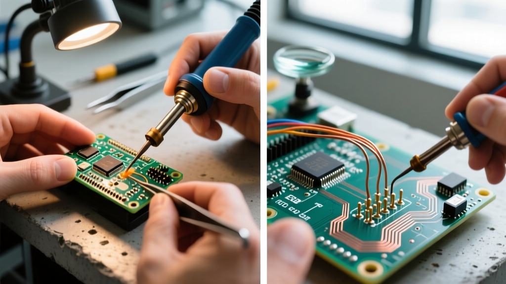
Search any major stock photo database for "soldering," and the top results will feature models holding the soldering iron like a kitchen knife. This "dagger grip" is physically impossible to use for precision PCB work. According to expert guides like SparkFun's Through-Hole Soldering Tutorial, the correct method requires a pencil grip. This allows the user to manipulate the iron with their fingers, achieving the critical 45-degree angle needed to simultaneously touch the component lead and the PCB pad. The dagger grip forces a steep, vertical approach, which often melts the component's plastic housing before the pad reaches flow temperature.
2. The Conical Tip Misrepresentation
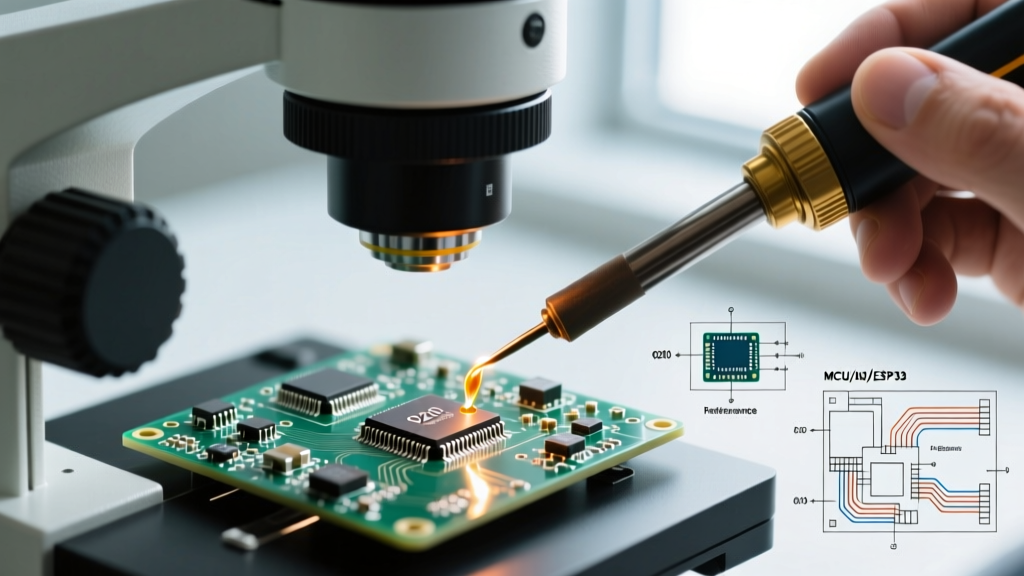
Stock photographers love conical (needle) tips because they look "precise" and high-tech to the untrained eye. In reality, conical tips are notoriously difficult to use for through-hole and standard SMD work because they offer a microscopic surface area for thermal transfer. Professional electronics assemblers rely on chisel or bevel tips. A 2.4mm chisel tip provides a broad thermal bridge, allowing the heat to flow rapidly into the copper pour. When a beginner mimics a stock photo and buys a conical tip, they inevitably experience thermal lag, leading to prolonged dwell times (exceeding the recommended 2-3 seconds per joint) and lifted pads.
3. "Painting" the Joint (The Solder Feed Error)
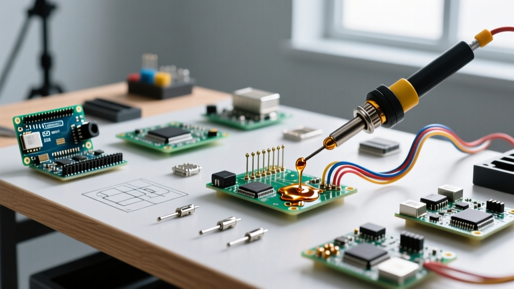
A hallmark of stock image soldering is the depiction of the user melting a glob of solder onto the iron tip, and then "painting" or wiping it onto the joint. This is a catastrophic error known as a cold or dry joint. The flux inside the solder core burns off the moment it touches the iron, leaving behind oxidized metal that will not metallurgically bond to the copper pad. The correct method dictates that the iron heats the workpiece (the pad and lead), and the solder wire is fed directly into the workpiece, not the iron. Stock images almost never capture this crucial thermodynamic sequence.
4. Spherical Beads and Non-Wetting
Visually, stock photos often highlight large, shiny, spherical balls of solder sitting on top of a pad. While this might look like "a lot of solder" to a layman, it actually demonstrates non-wetting. A proper IPC Class 2 or Class 3 solder joint must exhibit a concave fillet, where the solder flows smoothly up the component lead and feathers out onto the pad with a wetting angle of less than 90 degrees. Spherical beads indicate that the pad was not hot enough, the flux was exhausted, or the pad was contaminated with oxidation.
Expert Insight: "Visual learning is the primary vector for muscle memory in electronics assembly. If a beginner's first mental model of a solder joint is a spherical bead from a stock photo, they will subconsciously accept non-wetting as a successful connection, leading to latent field failures in their prototypes." — Senior IPC Certified Trainer
The Buyer’s Guide: Sourcing Visuals for Soldering Kits & Tutorials
For e-commerce sellers, technical writers, and hardware startups, the decision between licensing stock image soldering assets and investing in custom PCB photography comes down to long-term ROI and brand credibility.
Option A: Licensing Stock Image Soldering
- Cost: $5 to $25 per image via standard microstock platforms.
- Turnaround: Immediate download.
- Best Use Case: Generic blog headers, non-instructional marketing banners, or abstract conceptual articles about the electronics industry.
- The Risk: High. If used in instructional manuals or Amazon listing infographics, savvy hobbyists will immediately recognize the technical errors, destroying trust in your kit's quality. Furthermore, teaching bad habits results in negative reviews blaming your kit for the user's failed joints.
Option B: Commissioning Custom PCB Macro Photography
- Cost: $350 to $800 per day for a specialized macro product photographer, plus the cost of sacrificial PCBs and components.
- Turnaround: 2 to 4 weeks for shooting, lighting adjustments (managing reflections on flux and solder), and retouching.
- Best Use Case: Step-by-step assembly manuals, Kickstarter campaign visuals, premium Amazon A+ content, and technical troubleshooting guides.
- The ROI: Custom imagery featuring correct chisel tips, proper pencil grips, and beautiful concave IPC-compliant fillets drastically reduces customer support tickets. When a user can clearly see the exact wetting angle and flux residue expected, their confidence increases, and return rates for "defective kits" drop by an estimated 15-20%.
Final Verdict: Elevating the Visual Standard
The era of accepting technically illiterate stock image soldering in professional and educational spaces must end. As the DIY electronics community matures in 2026, consumers and learners are highly attuned to authenticity and technical rigor. While stock photos offer a cheap, immediate fix for empty web pages, they actively sabotage the transfer of knowledge. For any brand, educator, or platform serious about empowering makers, investing in custom, IPC-compliant photography is not just a marketing expense—it is a fundamental requirement for user success and product integrity.