
The Paradigm Shift: From Through-Hole to Surface Mount
The electronics manufacturing landscape underwent a seismic shift in the late 20th century, moving away from bulky through-hole technology (THT) toward the high-density, automated world of surface mount technology. Today, SMD SMT soldering is the undisputed backbone of global electronics production, enabling everything from ultra-compact IoT sensors to massive server motherboards. But this transition was not instantaneous. It required decades of metallurgical research, thermal engineering, and equipment innovation. Understanding the history and evolution of SMD SMT soldering provides critical context for modern PCB designers, DIY enthusiasts, and small-batch manufacturers navigating the equipment market today.
The Pre-SMT Era: Limitations of Through-Hole Technology
Before the widespread adoption of surface mount devices (SMDs), printed circuit boards (PCBs) relied on through-hole components. Leads were inserted into pre-drilled holes and secured using wave soldering. While robust and mechanically strong, THT presented severe limitations:
- Real Estate Constraints: Components could only be placed on one side of the board, and routing traces between drilled holes was a geometric nightmare.
- Drilling Costs: Drilling thousands of micro-holes per board was time-consuming, expensive, and prone to drill-bit breakage.
- Parasitic Inductance: The long leads of THT components introduced unwanted parasitic inductance and capacitance, severely limiting high-frequency and RF circuit performance.
As the aerospace and defense sectors demanded smaller, lighter, and more reliable electronics in the 1960s, the industry recognized that a fundamental change in component packaging and soldering methodology was required.
1960s-1980s: The Birth of Surface Mount Technology
The earliest iterations of SMD SMT soldering were pioneered by NASA and the U.S. military. The Apollo Guidance Computer, developed in the mid-1960s, utilized early surface-mount flat-pack integrated circuits to save crucial weight and volume. However, these early methods were highly manual and relied on specialized epoxies and hand-soldering under microscopes.
It was not until the 1980s that companies like IBM commercialized SMT for consumer and enterprise electronics. The introduction of automated pick-and-place machines and the development of solder paste—a thixotropic mixture of microscopic solder spheres and flux—allowed for mass reflow soldering. According to historical archives maintained by the Surface Mount Technology Association (SMTA), the 1980s saw SMT capture over 10% of the global PCB assembly market, a number that would skyrocket to over 90% by the early 2000s.
The Core Evolution of SMD SMT Soldering Methods
As component sizes shrank, the methods used to melt and reflow the solder paste had to evolve to prevent thermal shock, tombstoning, and cold joints.
1. Wave Soldering for SMD (The Transitional Phase)
Initially, manufacturers attempted to adapt existing THT wave soldering machines for SMDs. Components were glued to the bottom of the PCB using cyanoacrylate or UV-curable adhesives, passed through a fluxer, and dragged over a wave of molten tin-lead. This method suffered from the 'shadow effect,' where larger components blocked the solder wave from reaching smaller adjacent SMDs. By the late 1990s, wave soldering for pure SMD boards was largely abandoned in favor of reflow.
2. Infrared (IR) to Forced Convection Reflow
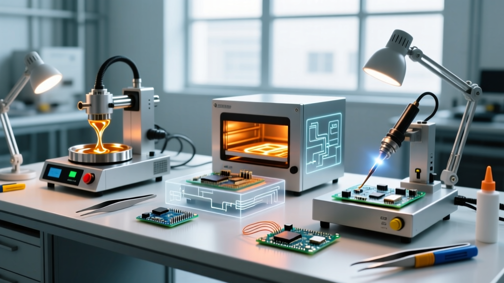
Early reflow ovens used infrared lamps to heat the boards. However, IR soldering was notoriously inconsistent; dark-colored components absorbed heat rapidly, while shiny or light-colored components reflected it, leading to uneven thermal profiles and burnt ICs. The industry evolved toward forced convection reflow ovens, which use heated air (often in nitrogen atmospheres to prevent oxidation) to uniformly transfer heat. Modern convection ovens feature 8 to 14 distinct heating zones, allowing precise execution of complex thermal profiles.
3. Vapor Phase Soldering
Vapor phase soldering uses an inert perfluoropolyether (PFPE) fluid, such as Galden, which boils at a specific temperature (e.g., 230°C for lead-free SAC305). When the PCB is lowered into the vapor blanket, it heats uniformly to the exact boiling point of the fluid, making it impossible to overheat the board. While largely relegated to niche, high-reliability aerospace applications due to the high cost of the fluids, vapor phase remains a fascinating branch of SMD SMT soldering evolution.
The RoHS Directive and the Lead-Free Thermal Challenge
The implementation of the Restriction of Hazardous Substances (RoHS) directive in 2006 forced the SMD SMT soldering industry to abandon eutectic Tin-Lead (Sn63/Pb37), which melted at a forgiving 183°C. The shift to SAC305 (Tin/Silver/Copper) raised the liquidus temperature to 217°C, demanding peak reflow temperatures of 245°C and forcing a complete redesign of thermal profiles and component packaging tolerances.
This temperature jump necessitated the adoption of Ramp-Soak-Spike (RSS) and Ramp-to-Spike (RTS) thermal profiles to ensure the flux volatiles boiled off before the solder melted, preventing solder balling and voiding inside BGA (Ball Grid Array) packages. For a comprehensive breakdown of modern acceptable solder joint criteria, engineers rely heavily on the IPC (Association Connecting Electronics Industries) and their IPC-A-610 standard.
Component Miniaturization and Solder Paste Evolution
The driving force behind SMD SMT soldering innovation has been the relentless miniaturization of passive components. As package sizes shrank, the particle size of the solder paste (classified by IPC J-STD-005) had to shrink proportionally to prevent bridging between micro-pads.
| Package Size (Imperial) | Dimensions (mm) | Required Paste Type | Particle Size Range | Primary Assembly Method |
|---|---|---|---|---|
| 1206 | 3.2 x 1.6 | Type 3 | 25 - 45 µm | Standard Convection Reflow |
| 0603 | 1.6 x 0.8 | Type 4 | 20 - 38 µm | Convection Reflow |
| 0201 | 0.6 x 0.3 | Type 5 | 15 - 25 µm | High-Precision Reflow / Laser |
| 01005 | 0.4 x 0.2 | Type 6 | 5 - 15 µm | Laser Soldering / Jet Printing |
| 008004 | 0.25 x 0.125 | Type 7 / Nano | 2 - 11 µm | Specialized Laser / Sintering |
Modern Lab Buying Guide: Equipping for SMD SMT Soldering Today
If you are setting up a prototyping lab or a small-batch production line in 2026, you do not need a $500,000 automated SMT line. The democratization of SMT equipment allows for highly capable benchtop setups. Here is a targeted buying guide for modern SMD SMT soldering workflows:
1. Stenciling and Paste Application
Skip the manual syringe dispensing for anything smaller than an 0805 package. Invest in a framed, electroformed nickel stencil ($150-$250 via services like PCBWay or Stencils Unlimited). For the fixture, a basic manual stencil printer like the FKM FP-250 ($300) provides the necessary Z-axis and XY micro-adjustments to align 0402 pads accurately. Use a high-quality Type 4 or Type 5 No-Clean SAC305 paste, such as Indium Corporation NC-D500 ($85 per 500g jar), keeping it refrigerated to prevent flux degradation.
2. Benchtop Reflow Ovens
For low-volume reflow, the NeoDen IN12 ($1,800) is an industry staple for small labs, featuring internal conveyor belts and 12 heating zones capable of profiling up to 280°C. For DIYers on a strict budget, the Whirlpool T962A ($250) is a popular entry point, though it heavily requires community-developed firmware mods and thermal tape upgrades to achieve reliable IPC-compliant lead-free profiles.
3. Precision Rework and Hand Soldering
Even with automated reflow, rework and prototyping require elite hand soldering tools. Standard chisel tips are useless for 0201 components.
- Hot Air Rework: The Quick 861DW ($280) offers exceptional airflow stability and rapid thermal recovery, crucial for lifting QFN and BGA chips without scorching the PCB laminate.
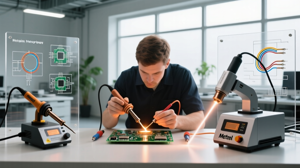
- Micro-Soldering Iron: For ultra-fine SMD SMT soldering, the JBC CD-2BQE station ($650) paired with C115-112 nano-tips is unmatched. JBC's cartridge-based heating element sits millimeters from the tip apex, delivering 130 watts of instantaneous thermal recovery, allowing you to drag-solder 0.4mm pitch TSSOP pins without thermal dragging.
- Bottom Preheating: To prevent board warpage and reduce the thermal shock to multilayer ceramic capacitors (MLCCs), use a bottom preheater like the Hakko FR-830 ($380). Holding the ambient board temperature at 120°C drastically reduces the hot air required from the top.
Conclusion
The evolution of SMD SMT soldering is a testament to the electronics industry's relentless pursuit of miniaturization and efficiency. From the crude glue-and-wave methods of the 1970s to today's nitrogen-inert convection ovens and nano-particle laser systems, the technology has continuously adapted to the shrinking footprint of silicon. For modern engineers and makers, understanding this history is not just an academic exercise; it informs the critical equipment and material choices required to yield reliable, high-density PCB assemblies in the modern era. Whether you are hand-soldering a 0402 resistor with a JBC nano-tip or profiling a 10-zone reflow oven for a BGA processor, you are participating in a continuous lineage of thermal and metallurgical innovation.
For further reading on historical electronics manufacturing standards, consult the archives at Wikipedia's Surface-Mount Technology Overview and the technical papers published by the SMTA.