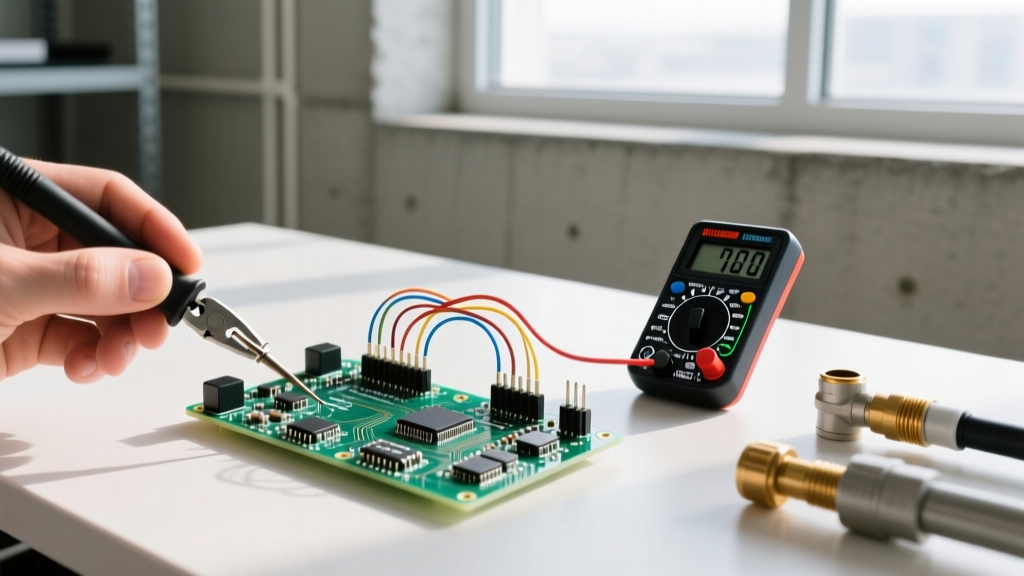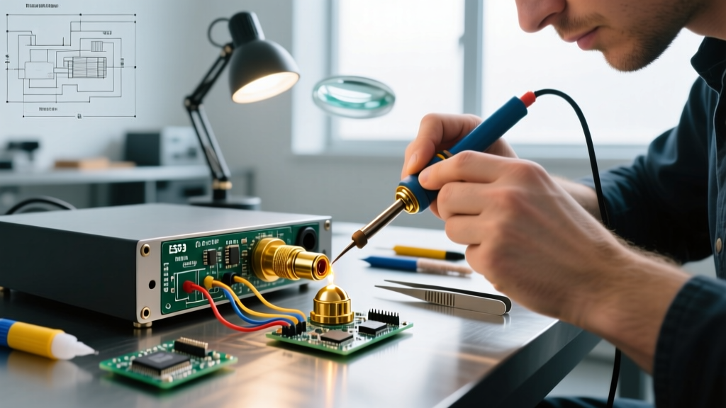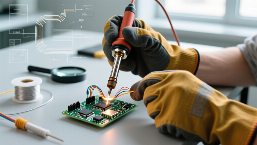

The landscape of electronics assembly and repair is defined by the materials you melt. Navigating the solders field requires more than just picking up a spool of wire; it demands a deep understanding of metallurgy, thermal dynamics, and application-specific requirements. Whether you are executing a Class 3 aerospace repair or prototyping a high-density IoT sensor, selecting the wrong alloy or mismanaging your thermal profile will result in catastrophic joint failure.
This guide cuts through the noise of the modern solders field, providing actionable FAQs, exact alloy specifications, and a rigorous troubleshooting matrix for the most common metallurgical defects encountered in 2026.
Core FAQ: Decoding the Solders Field
What is the real-world difference between SAC305 and SAC405?
In the lead-free solders field, SAC (Tin-Silver-Copper) alloys dominate. SAC305 (Sn96.5/Ag3.0/Cu0.5) is the baseline RoHS-compliant standard, melting between 217°C and 220°C. However, SAC405 (Sn95.5/Ag4.0/Cu0.5) contains an extra 1% silver. While this increases material costs by roughly 15-20%, that additional silver significantly improves drop-shock resistance and reduces the formation of brittle intermetallic compounds (IMCs) like Cu6Sn5 at the pad interface. If you are repairing portable field equipment subject to physical vibration, SAC405 or SAC305 doped with trace nickel (SAC305-Ni) is the superior choice.
Why is Sn63/Pb37 still relevant in a RoHS-dominated market?
Despite global environmental directives, Sn63/Pb37 (the eutectic leaded alloy melting at exactly 183°C) remains the undisputed king of mission-critical applications. According to NASA technical standards for soldered electrical connections, leaded alloys are still mandated for high-reliability spaceflight hardware to prevent tin whisker growth. The eutectic nature of 63/37 means it transitions from liquid to solid instantly without a plastic (pasty) phase, eliminating the risk of micro-cracking caused by component movement during cooling.
How do I select an alloy for low-temperature field repairs?
When repairing heat-sensitive components like RF modules or flexible PCBs in the field, standard SAC alloys will scorch the substrate. Enter Bismuth-doped alloys. Sn42/Bi57/Ag1 melts at a mere 138°C. It is exceptionally brittle on its own, but the 1% silver addition provides enough tensile strength for low-stress joints. Warning: Never mix Bismuth solder with leaded pads; the resulting ternary eutectic melts at 96°C and will fail at room temperature.
Troubleshooting Matrix: Solder Joint Failures
Visual inspection based on IPC-A-610 acceptability requirements is your first line of defense. Use this matrix to diagnose and correct joint failures.
| Defect Type | Visual Cue | Root Cause in the Solders Field | Corrective Action |
|---|---|---|---|
| Cold Joint | Dull, grainy, convex surface | Insufficient thermal transfer; tip temp too low for the alloy's liquidus point or ground plane mass. | Increase iron temp by 30°C. Switch to a bevel tip for surface area contact. Apply Kester 951 liquid flux to lower surface tension. |
| De-wetting | Solder pulls back, exposing base metal | Severe oxidation on the PCB pad or component lead; incompatible flux chemistry. | Clean pad with isopropyl alcohol and fiberglass pen. Switch from RMA (Rosin Mildly Activated) to RA (Rosin Activated) flux. |
| Solder Balling | Tiny spheres of solder clinging to flux residue | Flux boiling too violently, ejecting molten solder; or solder wire fed directly into the flame/iron tip rather than the joint. | Feed solder wire into the heated joint, not the iron tip. Lower iron temp by 15°C to prevent flux flash-boiling. |
| Disturbed Joint | Frosted appearance with visible micro-fissures | Component moved while the SAC alloy was in its "pasty" phase (between solidus and liquidus). | Use a eutectic alloy (Sn63/Pb37) if permissible, or employ a PCB preheater to slow the cooling curve. |
Field Repair Specifics: Overcoming Portable Challenges
Operating in the solders field outside of a climate-controlled lab introduces severe thermal variables. Wind, ambient temperature, and lack of heavy benchtop power supplies require specialized techniques.
Expert Insight: When using portable irons like the Pinecil V2 or TS101 in outdoor environments, the limiting factor is rarely the tip temperature—it is the thermal recovery rate. A 65W USB-C iron will stall when hitting a multi-layer PCB ground plane. Always use a portable 100W+ PD power bank to ensure the iron can sustain the current draw required to melt SAC305 on heavy copper pours.
Managing Thermal Mass in the Field
- Preheating: If you lack a benchtop preheater, use a high-wattage heat gun set to 120°C to bring the entire PCB up to temperature before applying your soldering iron. This reduces the delta-T the iron must overcome.
- Flux Selection: In high-humidity field environments, water-soluble fluxes can absorb ambient moisture and splatter. Stick to high-solids, no-clean tacky fluxes (like Amtech NC-559-V2-TF) which displace moisture and provide. Ensure the flux is stored in an airtight syringe to prevent solvent evaporation.
Advanced Metallurgical Considerations
As component sizes shrink to 0201 and 01005 imperial packages, the volume of solder deposited drops to microscopic levels. In these micro-BGA and ultra-fine-pitch scenarios, the metallurgical composition of your solder paste becomes critical.
Type 5 and Type 6 Solder Pastes
Standard Type 3 or Type 4 pastes (particle sizes ranging from 20-45 microns) will cause bridging on ultra-fine pitches. Navigating this niche of the solders field requires Type 5 (15-25µm) or Type 6 (5-15µm) powders. These finer powders have a vastly higher surface-area-to-volume ratio, meaning they oxidize much faster. If you are stencil printing Type 6 paste in a field repair scenario, you must use a nitrogen-rich environment or an aggressive halide-activated flux to prevent the powder from turning to dross before reflow.
Intermetallic Compound (IMC) Growth
Every time you rework a joint, the copper-tin IMC layer (Cu6Sn5 and Cu3Sn) grows thicker. While a thin IMC layer (1-2 microns) is necessary for a metallurgical bond, an IMC layer exceeding 5 microns becomes highly brittle and prone to thermal cycling fractures. If a pad has been reworked more than three times, the IMC layer has likely compromised the joint's structural integrity. The only proper fix is to abandon the pad and route a jumper wire.
Summary of Best Practices
Success in the solders field is not about memorizing every alloy; it is about matching the metallurgy to the mechanical and thermal demands of the specific application. Keep your tips tinned with a sacrificial layer of 63/37 to prevent iron plating dissolution, calibrate your thermal expectations based on the PCB's copper weight, and never compromise on flux chemistry. By applying these rigorous troubleshooting frameworks, you can ensure reliable, long-lasting electronic assemblies in any environment.