
The Critical Role of Soldering Tinning in High-Reliability Electronics
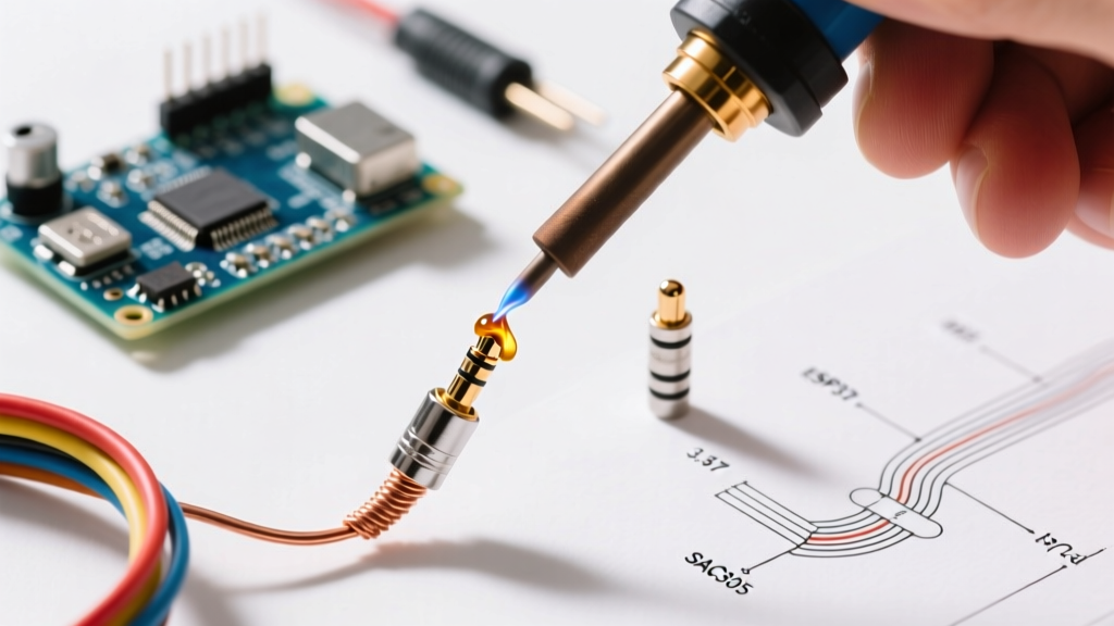
In professional electronics assembly and high-stakes DIY projects, soldering tinning is the foundational step that separates reliable, IPC-compliant joints from catastrophic field failures. Tinning—the process of pre-coating a wire, PCB pad, or soldering iron tip with a thin, uniform layer of molten solder—serves three vital purposes: it strips away microscopic oxidation, establishes the initial intermetallic compound (IMC) layer, and drastically reduces the thermal dwell time required during the final soldering operation.
According to the IPC J-STD-001 standards for soldered electrical and electronic assemblies, proper tinning ensures that stranded wires maintain their mechanical integrity and that surface mount pads are protected from environmental degradation before final component placement. In this comprehensive guide, we break down the metallurgy, precise temperature profiles, and 2026 buyer recommendations for mastering the tinning process.
The Metallurgy of Tinning: Understanding Intermetallic Compounds
When molten tin-based solder contacts a copper substrate (whether a bare wire or a PCB trace), it does not merely sit on the surface; it reacts metallurgically. This reaction forms an Intermetallic Compound (IMC). A properly tinned surface will exhibit two distinct IMC layers:
- Cu6Sn5 (Eta Phase): The primary layer that forms immediately upon contact. It is scalloped in structure and essential for a strong mechanical and electrical bond.
- Cu3Sn (Epsilon Phase): A secondary, thinner layer that forms between the copper and the Cu6Sn5 layer, primarily during prolonged heat exposure or long-term aging.
If you skip the tinning step and attempt to solder directly to oxidized copper, the flux must work overtime to clean the surface while the solder attempts to form the IMC layer simultaneously. This results in excessive heat application, melted wire insulation, and lifted PCB pads. Pre-tinning isolates the chemical cleaning phase from the final mechanical joining phase.
2026 Buyer Matrix: Essential Tinning Alloys & Supplies
Selecting the right solder alloy for tinning depends on your thermal budget and compliance requirements (e.g., RoHS). Below is a comparison of the most effective tinning alloys available in 2026, complete with current market pricing for standard 1 lb (454g) spools.
| Alloy Composition | Melting Point | Best Application | Avg. Price (2026) |
|---|---|---|---|
| Sn63/Pb37 (Eutectic) | 183°C (361°F) | Prototyping, aerospace (exempt), DIY | $45 - $55 |
| SAC305 (Sn96.5/Ag3.0/Cu0.5) | 217°C - 220°C | Commercial RoHS-compliant PCBs | $65 - $80 |
| Sn96.5/Sn3.0/Ag0.5 (Low-Ag) | 217°C - 220°C | High-volume automated tinning | $55 - $65 |
| Sn42/Bi57/Ag1 (Low-Temp) | 138°C - 174°C | Heat-sensitive components, step-soldering | $70 - $90 |
Pro Tip: For tinning iron tips, always use a dedicated tip tinner (like the Hakko 599B) which contains a highly activated flux and SAC305 solder powder designed to strip heavy oxidation without filing the tip.
Step-by-Step Tinning Protocols
1. Stranded Wire Tinning (AWG 22 to AWG 28)
- Strip the Wire: Remove exactly 3/16" to 1/4" of insulation for standard through-hole or terminal block connections. Ensure no copper strands are nicked.
- Mechanical Prep: Twist the strands tightly in the direction of the lay (usually clockwise). Do not over-twist, which can cause work-hardening and strand breakage.
- Apply Flux: Dip the twisted tip into a jar of Rosin Mildly Activated (RMA) or No-Clean liquid flux. Capillary action will wick the flux up into the strands.
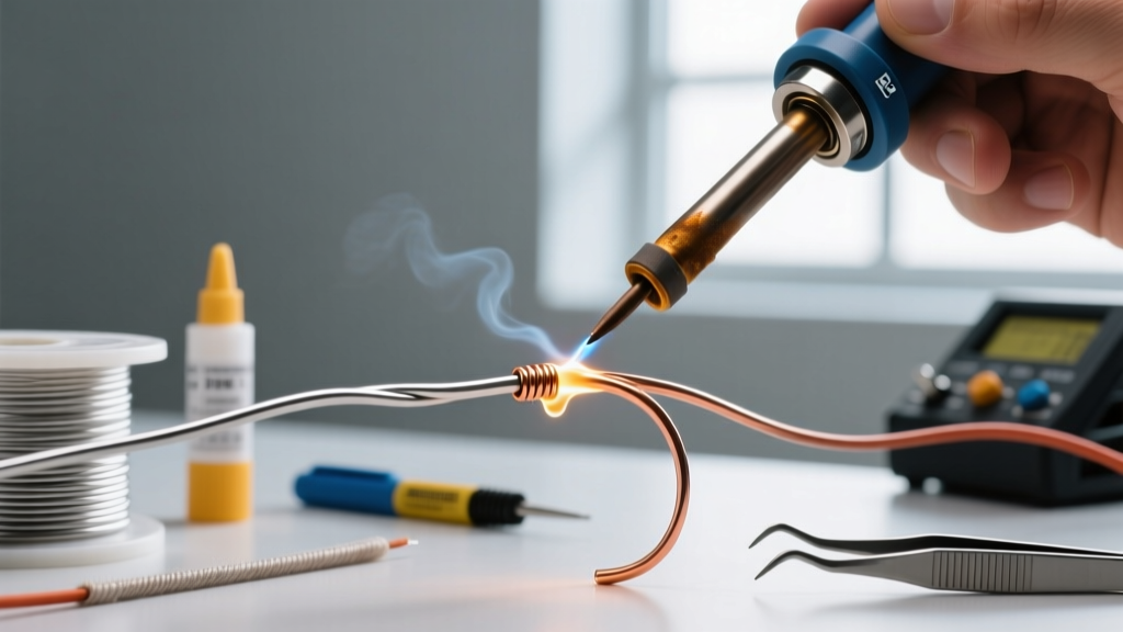
- Heat and Feed: Set your iron to 350°C (for Sn63/Pb37) or 380°C (for SAC305). Place the iron tip against the wire, wait 0.5 seconds for heat transfer, and touch the solder wire to the opposite side of the copper strand.
- Inspect: The solder should wick up to the insulation edge but not melt it back. The final tinned wire should show the contour of the individual strands (a "wetted" look), not a smooth, bulbous blob.
2. PCB Pad Tinning (Pre-Component Placement)
When repairing a board or prepping a bare PCB for heavy-gauge through-hole components, tinning the pads prevents oxidation during storage.
- Use a 1.6mm chisel tip for optimal thermal transfer to the ground planes.
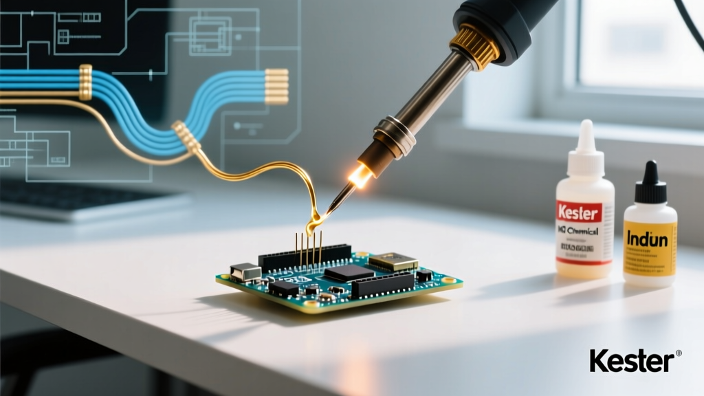
- Apply a generous amount of tacky flux (e.g., MG Chemicals 8341 or Amtech NC-559) directly to the pad array.
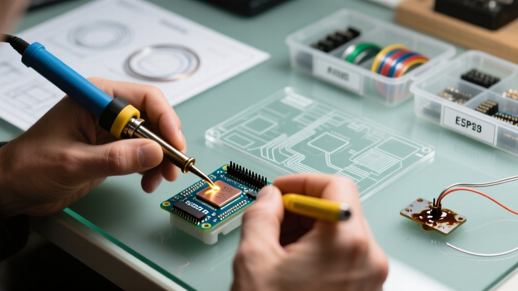
- Drag a pre-tinned iron tip across the pads at a 45-degree angle. The solder will instantly snap to the copper pads due to surface tension, leaving a flat, mirror-like finish.
3. Soldering Iron Tip Maintenance Tinning
The NASA Electronic Parts and Packaging (NEPP) workmanship guidelines emphasize that a soldering iron tip must never be left bare. The iron plating (typically 7 to 10 mils thick over a copper core) will rapidly oxidize at 380°C, leading to non-wetting and pitting.
Golden Rule of Tip Care: Never quench a hot tip in a soaking wet sponge. The rapid thermal shock causes micro-fractures in the iron plating, allowing molten solder to dissolve the copper core. Use a damp cellulose sponge or, preferably, a dry brass wire sponge (curling wool) to clean the tip, followed immediately by a thick coat of fresh solder before powering down.
Flux Chemistry: Matching Activators to Your Process
Tinning is impossible without flux. The flux removes copper oxide (CuO) and prevents re-oxidation while the solder is molten. According to IPC J-STD-004 classifications and formulations detailed by industry leaders like Chemtronics, you must select the correct flux chemistry for your tinning application:
- ROL0 / ROL1 (Rosin Low-Activity): Ideal for general-purpose wire tinning. Leaves a hard, non-conductive residue that is safe to leave on the board. Best for hobbyists and standard commercial repairs.
- REL0 / REL1 (Resin Low-Activity): Synthetic resin bases that offer better thermal stability than natural rosin. Excellent for high-temperature lead-free (SAC305) tinning processes where natural rosin would char and burn.
- ORG (Organic Acid / Water-Soluble): Highly aggressive. Used in industrial wire-tinning machines where the wire is subsequently washed in a DI water bath. Warning: Never use OA flux for PCB tinning unless you have a validated ultrasonic cleaning process, as residue will cause severe electrochemical migration (dendrite growth).
Troubleshooting Common Tinning Failure Modes
Even experienced technicians encounter tinning defects. Here is how to diagnose and correct the three most common failure modes:
Dewetting
Symptom: The solder initially wets the copper surface, but then pulls back into islands or droplets, exposing the bare metal underneath.
Cause: Contamination on the copper (silicone, machine oil, or conformal coating residue) or an excessively thick IMC layer formed by leaving the iron on the wire for too long.
Fix: Clean the wire with 99% isopropyl alcohol (IPA) and a lint-free swab. Re-strip the wire if the copper is heavily oxidized. Reduce dwell time to under 2 seconds.
Non-Wetting
Symptom: The solder balls up and rolls off the copper entirely, refusing to adhere.
Cause: Severe oxidation, insufficient heat, or inadequate flux activation.
Fix: Increase iron temperature by 15°C. Switch from a No-Clean flux to a mild Rosin Activated (RMA) flux to provide more chemical cleaning power. For PCB pads, lightly abrade the surface with a fiberglass scratch pen before re-fluxing.
Insulation Melt-Back
Symptom: The PVC or Teflon wire insulation shrinks, melts, or chars near the tinned joint.
Cause: Excessive dwell time, using an iron tip that is too massive for the wire gauge, or tinning the wire before twisting the strands (which traps air and slows heat transfer).
Fix: Always twist strands before tinning. Use a micro-pencil tip (e.g., 0.4mm) for AWG 28-30 wires, and ensure your iron's thermal recovery rate is high enough to prevent the operator from holding the tip in place for more than 1.5 seconds.
Summary: Building a Tinning-First Workflow
Integrating a rigorous soldering tinning protocol into your workflow is the single most effective way to improve joint reliability and reduce rework. By understanding the metallurgical IMC layers, selecting the appropriate 2026 alloy and flux chemistry, and adhering to strict thermal dwell times, you ensure that every wire and pad is primed for a flawless final connection. Whether you are building a custom drone flight controller or repairing industrial automation equipment, remember: a perfectly tinned surface makes the final solder joint a matter of simple capillary action, rather than a battle against oxidation.