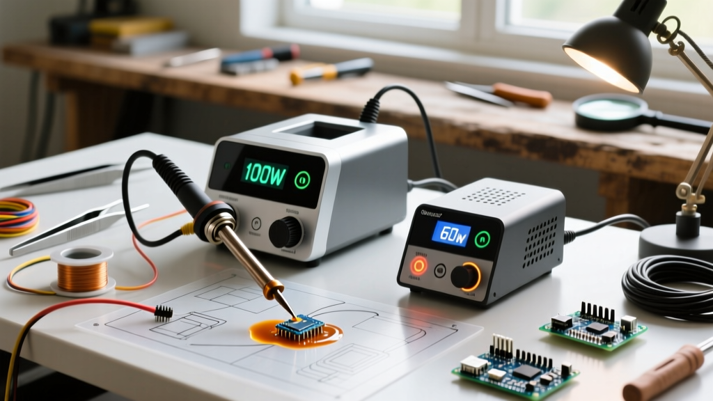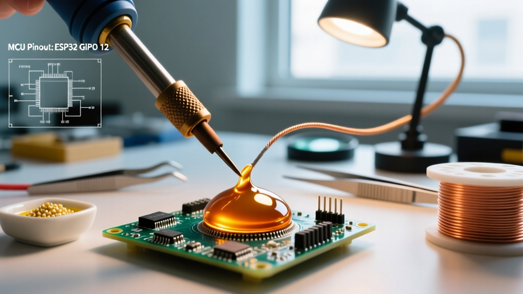

The Anatomy of the Perfect Soldering GIF
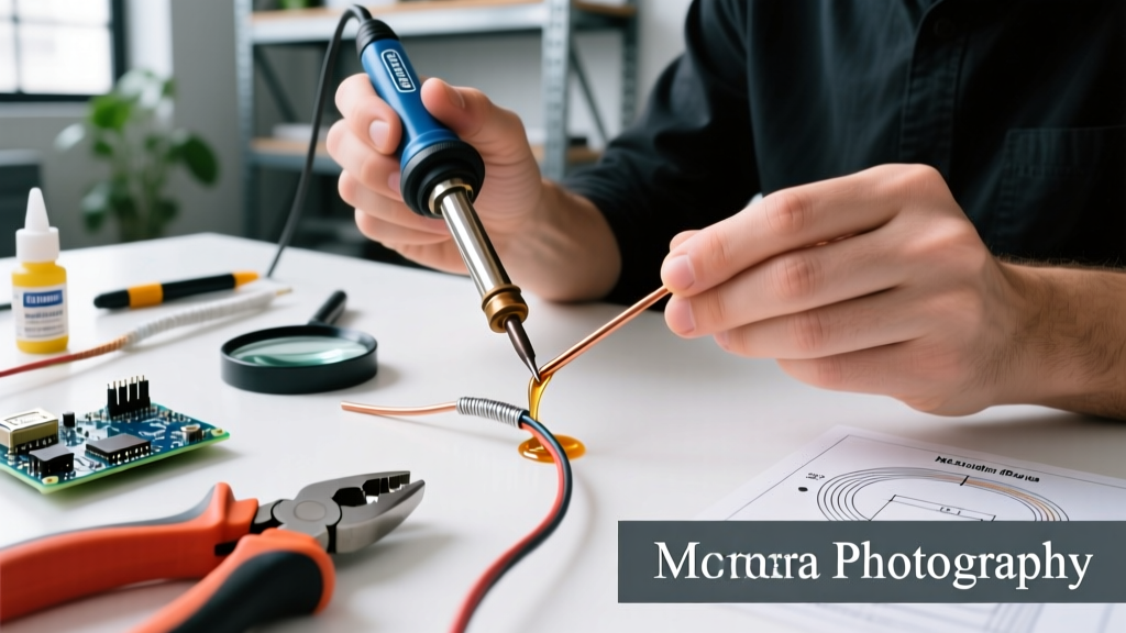
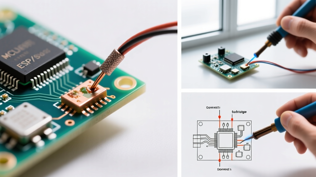
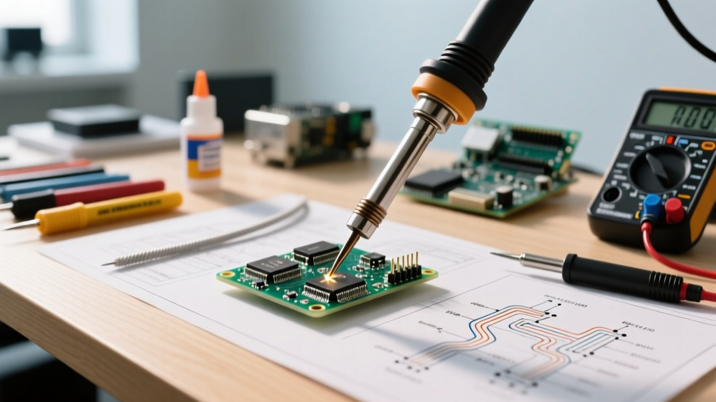
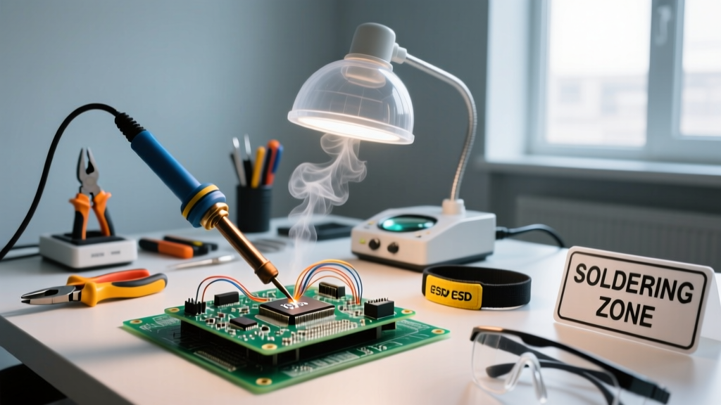
When technicians and hobbyists search for a 'soldering gif' online, they are usually looking for a quick visual reference of the perfect soldering technique. However, as a buyer and electronics professional in 2026, you should view these animated loops as much more than internet eye-candy. A high-quality soldering GIF is a masterclass in thermal dynamics, capillary action, and flux activation. By deconstructing the 3-second loop of a perfect joint formation, you can build a powerful visual decision framework to diagnose your current setup's flaws and make informed equipment purchasing decisions.
According to the NASA Workmanship Standards for electronic assemblies, the ideal solder fillet must exhibit a smooth, concave shape with a wetting angle of less than 90 degrees (and ideally under 30 degrees for through-hole components). When you watch a flawless soldering animation, you are witnessing the exact moment the solder alloy crosses its liquidus temperature, the flux boils off oxides, and the metallurgical bond forms. If your real-world results do not match the fluid dynamics seen in these visual references, it is time to use our decision framework to upgrade your gear.
Phase 1: Thermal Recovery and the 'Dwell Time' Decision
In any ideal soldering GIF, the solder wire touches the pad and the iron simultaneously, melting into a glossy puddle within 1.5 to 2.5 seconds. This metric is known as 'dwell time.' If your solder takes longer than 3 seconds to flow, or if it forms a dull, grainy blob before finally slumping into place, you are experiencing a thermal recovery failure.
Diagnosing the 'Cold Blob' vs. 'Smooth Fillet'
Modern 2026 PCB designs frequently utilize heavy ground planes and 0201 SMD components. These layouts act as massive heat sinks. When your iron's heating element cannot replenish the thermal energy lost to the board, the solder cools prematurely, resulting in a disturbed or cold joint. The IPC (Association Connecting Electronics Industries) strictly categorizes these grainy, disturbed joints as critical defects in Class 3 assemblies.
- The Visual Cue: Solder melts slowly, loses its mirror-like shine before the iron is removed, and forms a convex mound.
- The Diagnosis: Your station's thermal recovery rate (measured in Watts) is insufficient for the thermal mass of your target board.
- The Decision: It is time to abandon basic ceramic heater stations and invest in active-tip technology.
Phase 2: Flux Dynamics and Spatter Analysis
Watch the micro-explosions in a macro-level soldering GIF right before the solder flows. That spattering is the flux boiling and breaking down metal oxides. The behavior of this spatter dictates your consumable buying choices.
- Violent, Wide-Area Spatter: Indicates a water-soluble or highly activated flux encountering excessive heat (above 380°C). This can lead to corrosive residue that destroys traces over time.
- Gentle, Localized Bubbling: The hallmark of a high-quality No-Clean or Rosin Mildly Activated (RMA) flux operating in its ideal 300°C to 340°C window.
- No Spatter, Sudden Blackening: The flux core has burned off before the solder reached liquidus, usually due to an oversized iron tip or excessive dwell time.
Expert Insight: If your visual inspection reveals excessive spattering on adjacent pads, you are likely using a tip temperature that is 40°C too high for your specific flux core. Lowering the temperature and switching to a premium flux like Amtech NC-559-V2-TF will instantly improve joint cosmetics and reduce post-solder cleaning time.
The Visual Diagnostic Matrix
Use this decision matrix to translate the visual discrepancies between your real-world joints and the 'perfect' soldering GIF into actionable buying decisions.
| Visual Cue (The Missing GIF Frame) | Underlying Metallurgical Issue | Equipment / Consumable Decision |
|---|---|---|
| Solder balls up and refuses to flow onto the pad | Non-wetting due to severe oxidation or depleted flux core | Buy Kester 186 RMA liquid flux; replace oxidized iron tips immediately |
| Solder flows but looks dull, grainy, or frosty | Disturbed joint; thermal recovery failed during solidification phase | Upgrade to a JBC or Metcal station with active cartridge tips |
| Excessive black crust left on the tip after one joint | Flux carbonization from excessive tip temperature | Lower station temp by 30°C; buy a brass wool tip cleaner instead of a wet sponge |
| Solder wicks up the iron tip, refusing to touch the board | Heat gap; flux on the board hasn't activated to pull the solder down | Use a larger chisel tip to increase surface area contact; pre-tin the pad |
Phase 3: Upgrading Your Station Based on Visual Cues
If your soldering results consistently fail to match the fluid, glossy wetting action seen in professional reference media, your hardware is the bottleneck. Here is how to allocate your budget in 2026 based on the visual framework.
Budget Tier: Weller WE1010NA vs. Hakko FX-888D
For hobbyists and light repair work (through-hole and basic 0805 SMD), the visual cues of a failing joint usually point to slow thermal recovery rather than outright non-wetting. The Weller WE1010NA (priced around $125) offers a 70W heating element that recovers heat significantly faster than the legacy Hakko FX-888D ($105). While both are excellent entry-level stations, the Weller's digital interface and faster thermal response make it easier to maintain the 2.5-second dwell time required for a glossy fillet on moderate ground planes.
Pro Tier: JBC CD-2BQE and Active Tip Technology
If you are soldering 0402 components, heavy multilayer RF boards, or large power connectors, the visual gap between your work and the ideal reference is massive. You need active-tip technology. The JBC Tools Advanced Soldering Systems, specifically the JBC CD-2BQE station (retailing around $485 in 2026), places the heating element directly inside the tip cartridge.
This eliminates the thermal transfer gap found in traditional ceramic heaters. When the JBC tip touches a heavy copper pour, the station detects the temperature drop in milliseconds and delivers up to 130W of instantaneous power. The result? The exact 1.5-second melt and glossy wetting action you see in high-end production videos, regardless of the board's thermal mass.
Frequently Asked Questions
Why does my solder look shiny in the GIF but dull in real life?
A shiny joint indicates a smooth, undisturbed crystalline structure as the solder cooled from liquid to solid. If your joint is dull, the component or board moved microscopically during the 2-second cooling phase, or your iron's thermal recovery was so poor that the solder partially solidified while the iron was still applied. Secure your PCB in a heavy-duty vise (like a Panavise) and upgrade your station's wattage.
Can I use lead-free solder to achieve the same visual results as leaded solder?
Leaded solder (Sn63/Pb37) naturally produces a highly reflective, glossy fillet at lower temperatures (183°C liquidus). Lead-free alloys like SAC305 (217°C liquidus) inherently cool to a slightly duller, more satin finish. Do not mistake the natural satin finish of a properly wetted SAC305 joint for a cold joint. Judge lead-free joints by their concave shape and wetting angle, not just their mirror-like shine.
What is the best tip shape for mimicking professional wetting dynamics?
For 90% of general-purpose soldering, a 2.4mm chisel tip (such as the Weller ETA or Hakko T18-D24) provides the optimal balance of thermal mass and surface area contact. Conical tips (often included as stock tips on cheap stations) make point contact, severely limiting thermal transfer and causing the exact 'cold blob' failure mode you are trying to avoid.