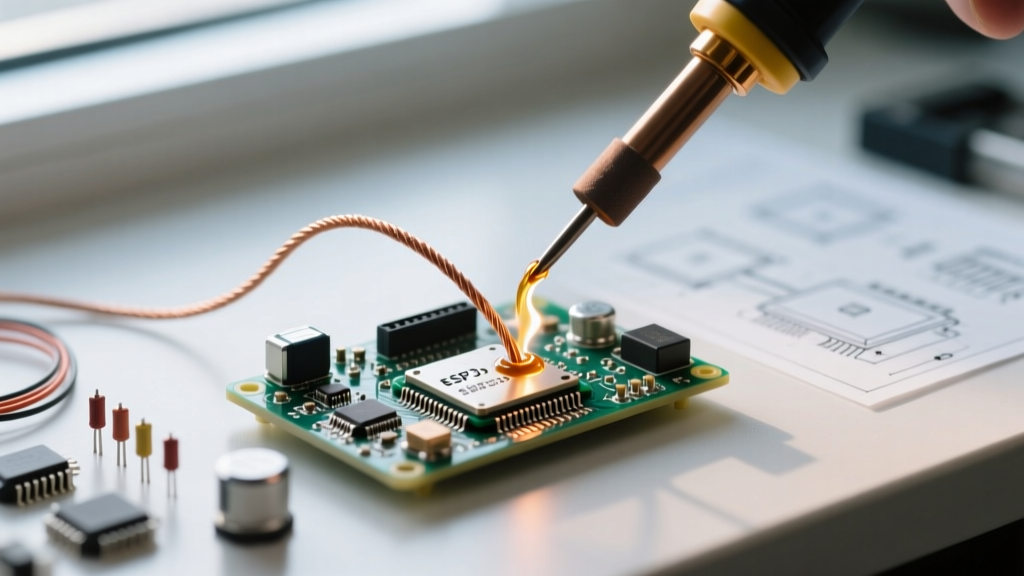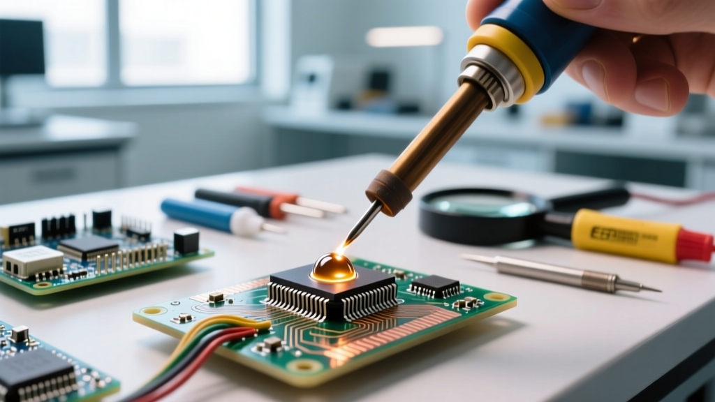

In the realm of high-reliability electronics—spanning aerospace, automotive ADAS, and medical life-support systems—the act of soldering a resistor transcends basic DIY assembly. It is a precise metallurgical bonding process governed by strict tolerances and rigorous quality standards. As we navigate the manufacturing landscape of 2026, miniaturization has pushed surface-mount device (SMD) resistors down to the 01005 imperial package size (0.4mm x 0.2mm), making the thermal dynamics of soldering a resistor more complex than ever before. Whether you are executing a manual rework on a satellite telemetry board or programming a reflow oven for high-volume automotive production, understanding the underlying physics and industry standards is non-negotiable.
The Physics of the Joint: Thermal Mass and Miniaturization
When soldering a resistor, the primary challenge is managing thermal mass disparities. A typical through-hole 1/4W carbon film resistor possesses a vastly different thermal profile compared to a 0402 or 0201 SMD thick-film resistor. In high-reliability applications, the goal is to achieve intermetallic compound (IMC) formation—specifically the Cu6Sn5 and Cu3Sn layers—without exceeding the thermal degradation threshold of the component or the PCB substrate.
For modern SMD resistors, the termination metallization is typically a nickel barrier layer with a matte tin or tin-lead outer plating. The nickel barrier prevents the underlying silver or copper from leaching into the solder bath, a phenomenon known as leaching or 'silver scavenging.' When soldering a resistor with a high-temperature lead-free alloy, the localized heat must be sufficient to melt the solder and wet the nickel barrier, but brief enough to prevent the PCB's FR-4 glass transition temperature (Tg) from being compromised, which can lead to pad lifting or delamination.
Material Selection: Alloys and Flux Chemistries
The choice of solder alloy and flux dictates the mechanical strength and long-term reliability of the joint. According to guidelines published by the Surface Mount Technology Association (SMTA), the industry has largely standardized around specific lead-free alloys for commercial and industrial applications, while aerospace and military sectors often retain leaded exemptions.
| Alloy Designation | Composition | Melting Point | Primary Industry Application |
|---|---|---|---|
| SAC305 | 96.5% Sn, 3.0% Ag, 0.5% Cu | 217°C - 220°C | Standard Commercial / Industrial SMD |
| SAC387 | 95.5% Sn, 3.8% Ag, 0.7% Cu | 217°C | High-Vibration Automotive (ADAS) |
| Sn63/Pb37 | 63% Sn, 37% Pb (Eutectic) | 183°C | Aerospace, Medical, Military (Class 3) |
| Sn96.5/Ag3.5 | 96.5% Sn, 3.5% Ag | 221°C | High-Temperature Downhole Drilling |
Flux Classification per IPC J-STD-004
Flux is the chemical engine that removes oxidation and enables wetting. For high-reliability PCB assembly, flux selection is categorized by material, activity level, and halide content. When soldering a resistor in a Class 3 environment (where equipment failure is life-threatening), ROL0 (Rosin, Low Activity, Zero Halides) is the gold standard. It provides sufficient cleaning action for mildly oxidized pads while leaving a benign, non-corrosive residue that does not require aggressive cleaning, thereby preventing ionic contamination that could lead to electrochemical migration (dendrite growth).
Hand Soldering Protocol for Leaded and SMD Resistors (IPC Class 3)
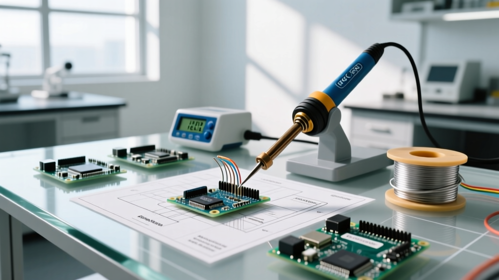
Manual soldering is frequently required for prototyping, low-volume high-reliability runs, and rework. The NASA Electronic Parts and Packaging (NEPP) Program and the IPC Standards dictate stringent procedures for hand soldering to ensure joint integrity. Below is the definitive protocol for soldering a resistor by hand to IPC-A-610 Class 3 requirements.
- Preparation and ESD Control: Secure the PCB on an ESD-safe workbench mat. Clean the target pads with >99% isopropyl alcohol (IPA) and a lint-free wipe. Apply a microscopic amount of ROL0 tack flux to the pads if performing rework.
- Tip Selection and Calibration: Select a tip geometry that matches the component's thermal mass. For 0603 or 0805 SMD resistors, a micro-pencil or narrow chisel tip (e.g., Weller RT4 or Metcal STTC-117) is ideal. For through-hole resistors, a larger chisel or conical tip with a wider surface area ensures rapid heat transfer. Calibrate the station to 350°C (662°F) for SAC305 lead-free solder, or 320°C (608°F) for Sn63/Pb37.
- Tinning and Heat Transfer: Lightly tin the tip with fresh solder to create a thermal bridge. Simultaneously touch the tip to the PCB pad and the resistor termination. Critical Rule: Never melt solder on the iron tip and carry it to the joint; the flux will burn off before the joint reaches wetting temperature.
- Solder Application and Dwell Time: Feed 63/37 or SAC305 wire solder (0.5mm diameter for SMD, 0.8mm for through-hole) directly into the junction of the pad, component lead, and iron tip. The solder should flow instantly via capillary action. Limit dwell time to a strict maximum of 2 to 3 seconds to prevent thermal damage to the resistor's internal ceramic substrate or epoxy coating.
- Fillet Formation and Cooling: Remove the solder wire first, then the iron. Allow the joint to cool naturally. Do not blow on the joint or use compressed air, as forced cooling can induce micro-cracking in the IMC layer. For Class 3 SMD resistors, the resulting joint must exhibit a smooth, concave fillet covering the toe, heel, and sides of the termination.
Automated Reflow: Soldering a Resistor at Scale
In high-volume manufacturing, soldering a resistor is accomplished via automated reflow ovens using solder paste (a suspension of microscopic solder spheres in flux). The thermal profile of the oven is meticulously engineered to accommodate the smallest and largest components on the board simultaneously.
Ramp-Soak-Spike (RSS) vs. Ramp-to-Peak (RTP)
For boards densely populated with varying component sizes, the RSS profile is preferred. It includes a 'soak' zone (typically 150°C to 180°C for 60-90 seconds) that allows the temperatures of high-thermal-mass components to equalize with low-thermal-mass SMD resistors before the final reflow spike. This prevents 'tombstoning'—a defect where one end of the resistor solders while the other lifts off the pad due to uneven surface tension caused by a thermal gradient.
Expert Insight on Tombstoning: When soldering a resistor adjacent to a large copper pour or a massive BGA component, the large mass acts as a heat sink, delaying the melting of the solder paste on the resistor's nearest pad. To mitigate this in 2026 PCB layouts, designers must employ thermal relief patterns on ground planes and ensure symmetrical trace routing to both pads of the SMD resistor.
Inspection, Testing, and Failure Mode Analysis
Following the soldering process, rigorous inspection is mandatory. Automated Optical Inspection (AOI) systems use high-resolution cameras and multi-angle lighting to verify joint geometry against IPC-A-610 Class 3 criteria. However, understanding failure modes is crucial for process engineers troubleshooting the line.
- Cold Solder Joints: Characterized by a dull, grainy, or lumpy appearance. Caused by insufficient heat transfer or movement during the cooling phase. In lead-free SAC alloys, this often manifests as a disturbed joint with visible crystalline fractures.
- Solder Wicking (Thievery): Occurs in through-hole or gull-wing SMD resistors when flux activation and heat cause the molten solder to travel up the component lead away from the pad, starving the joint of the necessary fillet volume.
- Pad Cratering: A catastrophic failure where the copper pad tears away from the FR-4 laminate, taking a small 'crater' of the resin with it. This is almost exclusively caused by excessive dwell times during hand soldering or mechanical stress applied to the resistor post-soldering.
- Solder Balls and Splatter: Tiny spheres of solder trapped under or beside the resistor body. This indicates moisture contamination in the solder paste or an excessively rapid ramp rate in the reflow oven, causing the flux solvents to boil violently and eject molten solder.
Industry Compliance and the Future of Resistor Assembly
As electronic systems become more autonomous and mission-critical, the margin for error in component assembly approaches zero. Soldering a resistor is no longer just about making an electrical connection; it is about ensuring mechanical resilience against thermal cycling, vibration, and long-term electromigration. By adhering to IPC J-STD-001 process requirements and IPC-A-610 acceptance criteria, manufacturers guarantee that every micro-ohm of resistance performs flawlessly in the field. Whether utilizing advanced vapor-phase reflow technology or executing precision hand-soldering under a microscope, the fundamental principles of thermal management, flux chemistry, and intermetallic formation remain the bedrock of reliable electronics manufacturing.