
The Critical Role of the Soldering Stencil in 2026 SMT Lines
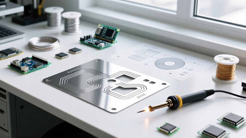
In modern Surface Mount Technology (SMT) manufacturing, the soldering stencil is the single most critical tool for determining first-pass yield. As the electronics industry in 2026 continues to shrink component footprints—with 01005 metric (0.4mm x 0.2mm) passives and 0.25mm pitch microBGAs becoming standard in telecommunications and automotive ADAS modules—the tolerance for stencil-induced defects is effectively zero. A poorly specified soldering stencil will cause catastrophic failure modes like solder bridging, tombstoning, and head-in-pillow (HiP) defects, costing high-volume facilities thousands of dollars per hour in rework and scrapped PCBs.
This comprehensive buyer and engineering guide details the material science, manufacturing methods, aperture design rules, and advanced nano-coatings required to specify the correct soldering stencil for your production environment.
Manufacturing Methods: Laser vs. Electroformed vs. Etched
The method used to cut the apertures into the stencil foil dictates the edge quality, which directly impacts solder paste release (transfer efficiency). Choosing the wrong manufacturing method for your component mix is a common procurement error.
| Manufacturing Method | Edge Quality & Release | Typical Cost (2026) | Best Application |
|---|---|---|---|
| Laser-Cut Stainless Steel | Good (requires electropolishing for fine-pitch) | $150 - $250 | Standard SMT, 0402/0603 passives, QFPs |
| Electroformed Nickel | Excellent (trapezoidal walls, superior release) | $350 - $600+ | Ultra-fine-pitch (UFP) BGAs, 01005, micro-SMT |
| Chemical Etching | Poor (hourglass profile, high paste retention) | $50 - $100 | Large through-hole pins, heavy power lugs |
| Laser-Cut Polyimide (Kapton) | Fair (flexible, prone to tearing) | $20 - $45 | Rapid prototyping, low-volume R&D runs |
For high-reliability manufacturing, Surface Mount Technology Association (SMTA) case studies consistently show that electroformed nickel stencils provide the highest transfer efficiency (often exceeding 90%) due to their naturally trapezoidal aperture walls, which act as a funnel to push solder paste onto the PCB pad.
Material Science and Thickness Specifications
Stencil thickness dictates the Z-axis volume of the solder paste deposit. In 2026, the industry standard for mixed-technology boards utilizes a baseline thickness of 4 mil (100µm) to 5 mil (125µm). However, the proliferation of bottom-terminated components (BTCs) and QFNs requires precise volume control to prevent solder extrusion and shorting under the thermal pad.
Stainless Steel Grades: 304 vs. 316
Most laser-cut stencils are manufactured from 304-grade stainless steel. However, for high-tension framing (above 35 N/cm) required by automated inline stencil printers, 316-grade stainless steel or specialized alloys like FG (Fine Grain) are preferred. FG alloys offer superior tensile strength, preventing the stencil from stretching and losing registration with the PCB pads over thousands of print cycles.
Step Stencils (Multi-Level Designs)
When a single PCB requires both massive solder volumes for large ground planes and microscopic volumes for 01005 components, engineers must specify a step stencil. Using a chemical milling or precision laser-welding process, the stencil foil is stepped down to 3 mil (75µm) in the microBGA zones, while remaining at 5 mil (125µm) for large connectors and power inductors. Expect to pay a 40% to 60% premium for step stencils, but the reduction in rework justifies the cost in high-volume runs.
IPC-7525 Compliance: Mastering Aspect and Area Ratios
The Association Connecting Electronics Industries (IPC) publishes the IPC-7525 standard, which provides the mathematical framework for stencil aperture design. To ensure reliable paste release from the stencil aperture to the PCB pad, manufacturing engineers must calculate two critical metrics:
The 0.66 Area Ratio Rule: For standard solder pastes (Type 3 or Type 4), the Area Ratio (AR) must be greater than 0.66 to guarantee reliable paste transfer. For advanced Type 5 or Type 6 powders used in 2026 micro-electronics, an AR > 0.55 may be acceptable, but > 0.66 remains the gold standard for six-sigma yields.
- Aspect Ratio (AR): Calculated as Aperture Width / Stencil Thickness. Must be > 1.5.
- Area Ratio (AR): Calculated as (Aperture Area) / (Aperture Perimeter × Stencil Thickness). Must be > 0.66.
If your component pad geometry results in an Area Ratio below 0.66, you must either reduce the stencil thickness locally (step stencil) or increase the pad size on the PCB footprint—a change that requires collaboration with the layout engineering team.
Aperture Reduction and Shape Modification
Simply cutting the aperture to the exact 1:1 ratio of the PCB pad is a recipe for disaster. Solder paste expands slightly during the reflow profile's liquidus phase. To prevent solder beading and bridging, stencils are designed with aperture reductions.
Common Aperture Shapes for Passives
- Home-Plate Cut: Reduces the inner edge of the pad by 10-15%. This pulls the solder paste mass toward the center of the pad during reflow, utilizing surface tension to prevent tombstoning (where one end of a capacitor lifts off the pad).
- U-Shape / V-Shape Cut: Used for large thermal pads on QFNs and LGAs. The large square pad is divided into a grid of smaller U-shaped or square apertures, creating a window-pane effect. This allows flux gases to escape through the unprinted channels, preventing voiding rates from exceeding the IPC Class 3 limit of 25%.
Nano-Coatings and Surface Treatments
In 2026, raw stainless steel is rarely used without surface modification for fine-pitch applications. The surface roughness (Ra) of the aperture walls creates friction, causing solder paste to stick to the stencil rather than transferring to the board.
Electropolishing is an electrochemical process that removes the microscopic burrs left by laser cutting, reducing Ra and improving transfer efficiency by 10-15%. For Type 5 and Type 6 solder pastes, which contain microscopic solder spheres prone to clinging to metal walls, Nano-coatings (such as NanoSlic or Phase Shift) are mandatory. These hydrophobic and oleophobic coatings alter the surface tension of the stencil, forcing the paste to release cleanly. A high-quality nano-coating adds $40 to $80 to the stencil cost but extends the time between automated stencil under-wipe cycles from every 3 prints to every 10 prints, drastically increasing line throughput.
2026 Procurement Guide: Pricing and Framing
When ordering from industrial stencil fabricators, you must specify the framing requirements. Loose foil is only for manual, low-tension R&D jigs. Automated printers like the DEK Horizon, MPM Momentum, or EKRA X6 require rigid frames.
- Standard Frame Sizes: 29" x 29" (736mm x 736mm) is the global standard for high-volume lines. 23" x 23" and 20" x 20" are common for smaller benchtop printers.
- Mesh Tension: Specify 30 N/cm to 40 N/cm. Tensions below 30 N/cm will cause gasketing failures (paste bleeding under the stencil).
- Cost Expectations: A fully framed, laser-cut, electropolished 29x29 stencil with nano-coating typically ranges from $220 to $350 in 2026, depending on the aperture count and data complexity.
Troubleshooting Stencil-Induced Solder Defects
Even with perfect data, process variables can cause defects. Here is how to diagnose stencil-related failures on the SMT line:
1. Solder Bridging (Shorts)
Cause: Apertures are too large, or the stencil is too thick, causing adjacent paste deposits to merge during reflow. Solution: Apply a 10% to 20% area reduction to the aperture. If using a 5 mil stencil, step down to 4 mil in the fine-pitch zones.
2. Gasketing (Paste Bleed)
Cause: The stencil is not sealing flush against the PCB during the print stroke. This is often caused by inadequate mesh tension (< 30 N/cm) or a warped PCB. Solution: Increase squeegee pressure slightly, but more importantly, verify stencil tension with a tensiometer. Retension or replace the stencil if it has fatigued past 25,000 print cycles.
3. Insufficient Paste Volume
Cause: Poor transfer efficiency due to rough aperture walls, incorrect Area Ratio (< 0.66), or clogged apertures from dried flux. Solution: Verify your under-stencil wipe frequency and solvent (use IPC-approved cleaning agents as recommended by metallurgical experts at AIM Solder). If wiping is adequate, upgrade to an electroformed stencil or apply a nano-coating.
Final Procurement Checklist for Manufacturing Engineers
Before sending your Gerber or ODB++ stencil data to the fabricator, ensure you have verified the following:
- Apertures are reduced by 10-15% for standard passives to prevent tombstoning.
- Thermal pads on QFNs/BTCs are window-paned (divided into a grid) to prevent voiding and solder extrusion.
- Area Ratios for all fine-pitch components are calculated and verified to be > 0.66.
- Step-down zones are clearly marked in the CAD data for mixed-height component boards.
- Nano-coating is specified if Type 5 or Type 6 solder paste is utilized in your BOM.
By treating the soldering stencil not as a mere consumable, but as a precision-engineered tool, manufacturing engineers can secure the high first-pass yields required to remain competitive in the demanding 2026 electronics market.