
The Fundamental Divide: Paste vs. Molten Pool
Choosing between reflow soldering and wave soldering is not a matter of identifying a universally superior technology; rather, it is an exercise in matching the soldering physics to your specific Bill of Materials (BOM) and production volume. In modern electronics manufacturing, the decision framework hinges on component density, thermal mass variations, and the ratio of Surface Mount Technology (SMT) to Through-Hole Technology (THT) parts. As we navigate the 2026 manufacturing landscape, where miniaturization (01005 and 008004 components) coexists with high-power THT connectors, understanding the exact operational boundaries of each method is critical for yield optimization.
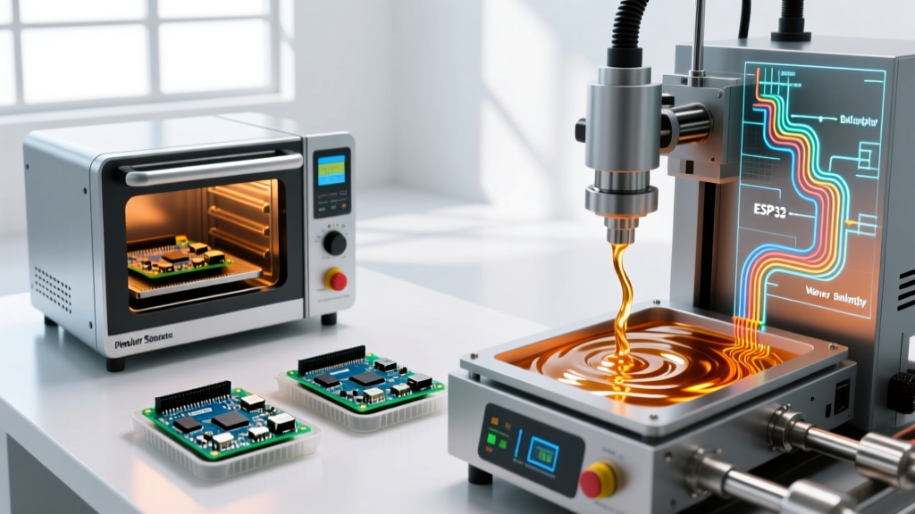
Core Principle: Reflow soldering relies on pre-applied solder paste and controlled thermal profiling to reflow localized joints. Wave soldering utilizes a continuous pump-driven wave of molten bulk solder to wet exposed pads and plated through-holes simultaneously.
The PCB Assembly Decision Matrix
Use the following matrix to determine the primary soldering method for your next production run. This framework evaluates the physical and economic constraints of both processes.
| Parameter | Reflow Soldering | Wave Soldering |
|---|---|---|
| Primary Component Type | SMT (BGA, QFN, 0402, 0201) | THT (Connectors, Transformers, DIP ICs) |
| Thermal Stress | Controlled (Ramp-Soak-Spike profile) | High (Direct molten contact, requires preheat) |
| Fine Pitch Capability | Excellent (Down to 0.3mm pitch) | Poor (Bridging risk below 0.8mm pitch) |
| Setup & Tooling Cost | Stencil ($150-$300), Fixture ($50) | Durostone Pallets ($250-$600 per SKU) |
| Consumables | Solder Paste (Type 4/5), Stencil wipes | Bulk Solder Bar, Liquid Flux, Dross removal |
| Ideal Volume | Medium to High (Automated Pick & Place) | High Volume THT or Mixed-Tech Palletized |
Deep Dive: Reflow Soldering Parameters & Failure Modes
Reflow soldering is the undisputed standard for high-density SMT boards. The process requires precise stencil design and thermal profiling. According to IPC-7525 guidelines, stencil thickness must be matched to component pitch: a 4-mil (100 µm) stencil is standard for fine-pitch QFNs and 0402s, while 5-mil is preferred for larger terminations to ensure adequate solder volume.
Critical Thermal Profiling
For standard lead-free SAC305 (Sn96.5/Ag3.0/Cu0.5) paste, the liquidus temperature is 217°C. A robust Ramp-to-Peak profile must achieve a peak temperature of 240°C–245°C, maintaining a Time Above Liquidus (TAL) of 45 to 60 seconds. Insufficient TAL results in cold, grainy joints, while excessive TAL degrades the flux chemistry and risks intermetallic compound (IMC) overgrowth, leading to brittle fractures under mechanical stress.
Edge Cases and Failure Modes
- Tombstoning: Prevalent in 0402 and 0201 passives. Caused by uneven wetting forces due to asymmetric pad heating or uneven paste deposition. Solution: Optimize pad geometry to IPC-7351B standards and ensure thermally balanced trace routing.
- Head-in-Pillow (HiP):strong> A notorious BGA failure mode where the component ball and paste deposit reflow but fail to coalesce. Often caused by flux exhaustion due to excessive preheat times or PCB warpage during the TAL phase.
- Solder Balling: Micro-splattering near pads, typically resulting from moisture absorption in the paste or an overly aggressive initial ramp rate (>3°C/sec) causing volatile flux solvents to boil explosively.
Deep Dive: Wave Soldering Dynamics & Edge Cases
Wave soldering remains indispensable for power electronics, automotive ECUs, and industrial control boards heavily populated with THT components. The process involves three distinct stages: fluxing, preheating, and wave contact. Industry experts at SMTNet frequently emphasize that 80% of wave soldering defects originate in the preheat and fluxing stages, not the wave itself.
Fluxing and Preheat Physics
Liquid flux (typically VOC-free or low-VOC rosin-based) must be applied uniformly via ultrasonic nozzles. The preheat zone is critical: it must raise the PCB's topside temperature to 90°C–110°C before the board hits the 260°C molten wave. This prevents thermal shock, minimizes PCB warpage, and activates the flux to deoxidize the copper pads and component leads.
Edge Cases and Failure Modes
- Solder Bridging: Highly common on SOIC or DIP ICs if the board's conveyor speed is too slow or the solder pot temperature drops below 255°C. Utilizing a 'chip wave' (turbulent wave) followed by a 'lambda wave' (laminar flow) helps peel excess solder away from tight pitches.
- Icicles and Webbing: Occurs when the solder's surface tension fails to break cleanly from the pad. Often a symptom of degraded flux activity or insufficient conveyor angle (standard is 6° to 8°).
- Flux Entrapment: If the preheat is inadequate, liquid flux can become trapped under components or inside vias, vaporizing upon contact with the wave and causing micro-splatter or internal voids in the barrel fill.
Navigating Mixed-Technology Boards (SMT + THT)
The most complex decision framework arises when a single PCB features both dense SMT microcontrollers and heavy THT power connectors. You cannot simply pass a fully populated mixed-tech board through a wave solder machine; the molten wave will destroy sensitive SMT plastics and wash away small passives.
The Standard Workflow:
- Phase 1: Apply solder paste via stencil, place all SMT components, and run through the reflow oven.
- Phase 2: Insert THT components. Secure SMT components on the bottom side using high-temperature Kapton tape or specialized SMT adhesives if they will be exposed to the wave.
- Phase 3: Run the board over the wave solder machine using a custom-machined Durostone pallet. The pallet shields the bottom-side SMT components from the molten solder while exposing only the THT leads through precision-cut apertures.
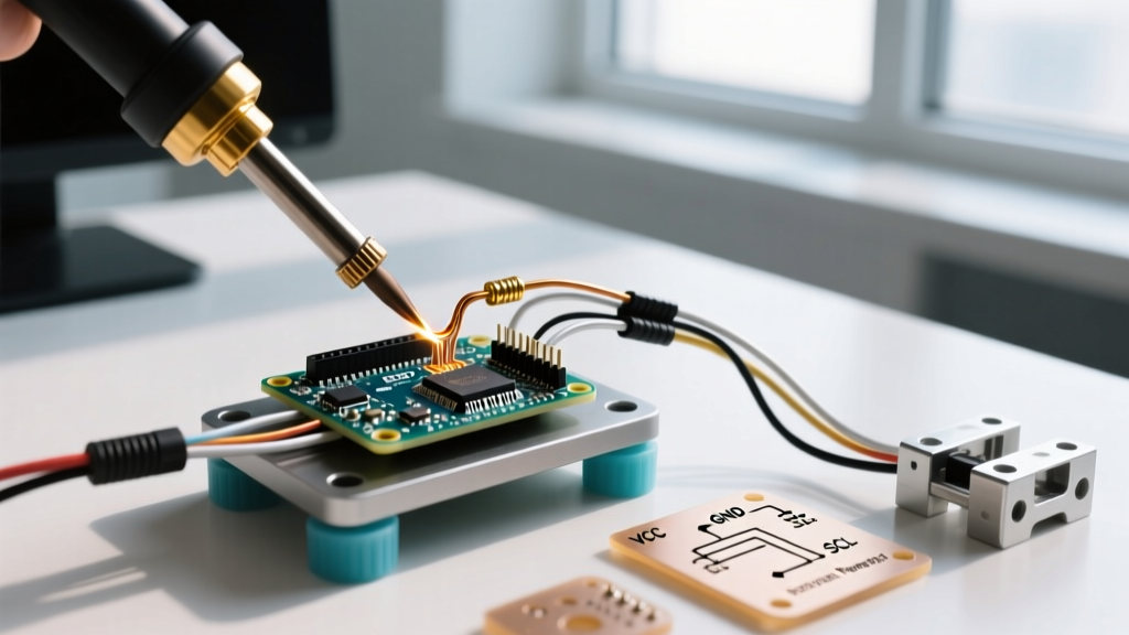
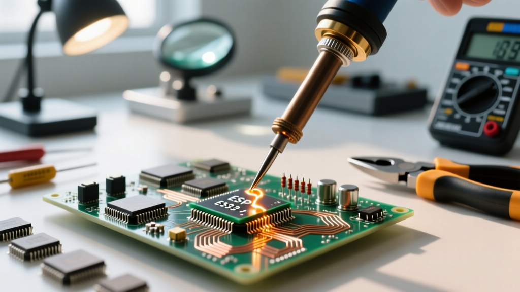
Alternative for Low Volume: For prototyping or runs under 50 units, skip the wave solder entirely. Reflow the SMT components first, then utilize selective wave soldering (a robotic micro-nozzle that solders individual THT pins) or high-quality hand soldering with a temperature-controlled iron (e.g., Weller WE1010 or JBC CD-2BQE) set to 350°C for THT joints.
Capital Expenditure and Consumable Costs (2026 Outlook)
When building an in-house assembly line or evaluating an EMS partner, the financial footprint of each method differs drastically. Reflow requires high upfront automation but boasts low marginal costs per board. A mid-range convection reflow oven (e.g., Heller 1809) costs upwards of $45,000, but the primary ongoing cost is solder paste (approx. $0.15 per board) and stencil maintenance.
Wave soldering machines (like the ERSA Powerflow series) carry a similar capital cost ($50,000–$80,000), but the consumable overhead is significantly higher. Lead-free SAC305 solder bars cost approximately $25 to $35 per pound. Furthermore, the oxidation process generates 'dross'—a slag of oxidized tin that must be skimmed and recycled. A high-volume wave machine can generate 10-20 lbs of dross per shift, representing a continuous material loss that must be factored into your unit economics. Additionally, nitrogen inerting systems are now standard in 2026 to reduce dross formation by up to 70%, adding to the initial infrastructure cost but yielding long-term ROI.
Final Verdict: Applying the Framework
Choose reflow soldering when your design is heavily SMT, requires fine-pitch routing (<0.65mm), and demands strict thermal profiling to protect sensitive silicon. Choose wave soldering when your BOM is dominated by THT components, requires high mechanical strength for board-edge connectors, and justifies the cost of custom palletizing. For mixed-technology boards, a hybrid approach—reflow first, followed by selective wave or palletized traditional wave—is the only reliable path to achieving IPC-A-610 Class 3 reliability standards without compromising component integrity.