
Decoding the 'Mad Solder' Phenomenon in Industrial PCB Assembly
When assembly line technicians and process engineers search for a real foto of mad solders, they are rarely looking for artistic macro photography. In the high-reliability electronics manufacturing sector, 'mad solder' is a prevalent piece of shop-floor slang used to describe wildly erratic, severely deformed, or non-wetting solder joints that defy standard reflow expectations. These visual anomalies—ranging from severe graping to catastrophic head-in-pillow (HiP) defects—are critical red flags in IPC-A-610 Class 3 environments.
As we navigate the manufacturing landscape of 2026, the miniaturization of components (such as 01005 and 008004 passives) and the widespread adoption of complex bottom-terminated components (BTCs) have made these erratic solder defects more common. Understanding the root causes behind these 'mad' visual anomalies is the first step toward engineering robust reflow profiles and selecting the right automated optical inspection (AOI) equipment.
The IPC-A-610 Standard: Defining 'Mad' vs. Acceptable
The IPC-A-610 standard does not use the term 'mad.' Instead, it categorizes defects based on wetting angles, fillet shapes, and intermetallic compound (IMC) formation. What a technician might call a 'mad' joint is typically classified under severe defect conditions:
- Non-Wetting: The solder fails to form a metallurgical bond with the base metal, resulting in a high contact angle (greater than 90 degrees) and a bead-like appearance.
- De-Wetting: The solder initially wets the surface but then recedes, leaving behind irregular, web-like islands of solder separated by exposed pad.
- Excessive Voiding: In Ball Grid Arrays (BGAs), internal gas entrapment creates voids that exceed the 25% threshold for Class 3 high-reliability products, leading to erratic X-ray signatures.
Industry Insight: According to the Surface Mount Technology Association (SMTA), over 65% of field failures in automotive and aerospace PCBs can be traced back to latent solder joint defects that bypassed 2D visual inspection but would have been caught by advanced 3D metrology.
Visual Breakdown: Real Fotos of the Worst Offenders
If you were to compile a gallery of the most severe solder defects, three specific anomalies consistently dominate the 'mad solder' category. Here is a deep dive into their visual characteristics and root causes.
1. Graping (Solder Balling and Cluster Defects)
The Visual: Instead of a smooth, concave fillet, the solder paste forms a cluster of semi-spherical balls that resemble a bunch of grapes. The flux has completely burned off or failed to activate, leaving the solder particles oxidized and uncoalesced.
Root Cause: Graping is heavily associated with lead-free SAC305 (Sn96.5/Ag3.0/Cu0.5) pastes, particularly Type 4 and Type 5 powder sizes used for micro-BGAs. In 2026, the primary culprit is flux exhaustion during an overly aggressive Ramp-Soak-Spike (RSS) reflow profile. The volatile solvents evaporate too quickly, and the rosin-based activators oxidize before the solder reaches its 217°C liquidus temperature.
Corrective Action: Transition to a Ramp-to-Peak (RTP) profile to minimize the time the flux is exposed to high heat before coalescence. Ensure your stencil aperture reduction is optimized to prevent excessive paste volume in micro-pads.
2. Head-in-Pillow (HiP) Defects
The Visual: In a cross-section or X-ray 'foto', a BGA sphere appears to be resting perfectly on top of the solder paste deposit without merging. The sphere and the paste look like a head resting on a pillow.
Root Cause: HiP is a nightmare for high-density server boards. It occurs when the PCB or the BGA substrate warps during the reflow process (often exceeding 0.5mm of deflection). The solder paste melts, but the BGA sphere lifts away due to thermal expansion mismatch. When the board cools and flattens, the sphere drops back onto the now-solid paste, creating a mechanical but not metallurgical connection.
Corrective Action: Utilize edge-support tooling in the reflow oven to minimize PCB warpage. Additionally, switching to a solder paste with a highly active, halogen-free flux chemistry can help break through the oxide layer on the BGA sphere during the brief moment of contact.
3. Tombstoning on Micro-Passives
The Visual: A surface-mount resistor or capacitor stands completely upright on one end, resembling a tombstone. The other pad is left with a pristine, undisturbed solder deposit.
Root Cause: This is a surface tension imbalance. On 0201 and 01005 components, if one pad heats up faster than the other (due to unequal thermal mass or trace routing), the solder on the hotter pad melts first. The surface tension of the liquid solder pulls the component upright before the second pad reaches liquidus.
Corrective Action: Implement home-genic pad designs and ensure symmetrical trace routing to both pads. In the reflow oven, reduce the conveyor speed and lower the peak temperature slightly to allow the entire board to reach thermal equilibrium before the solder transitions to a liquid state.
2026 Inspection Matrix: Catching the Unseen
You cannot rely on manual visual inspection to catch these 'mad' solder defects, especially with the rise of hidden joints in QFNs and LGAs. Industrial buyers must invest in automated inspection. Below is a comparison of the leading inspection technologies utilized in modern SMT lines.
| Inspection Technology | Primary Use Case | Defect Catch Rate (Hidden Joints) | Est. 2026 Capital Cost | Throughput Impact |
|---|---|---|---|---|
| 2D AOI | Polarity, missing components, basic bridging | < 10% | $45,000 - $70,000 | High (Fastest) |
| 3D AOI | Coplanarity, graping, tombstoning, volume check | ~ 40% (via side-view cameras) | $110,000 - $160,000 | Medium |
| 3D AXI (X-Ray) | BGA HiP, QFN voiding, internal barrel cracks | > 98% | $220,000 - $350,000+ | Low (Bottleneck risk) |
| Inline CT Scan | Aerospace/Medical Class 3 void analysis | 100% | $500,000+ | Very Low (Offline/Sampling) |
For high-mix, high-reliability manufacturers, a combined 3D AOI and selective 3D AXI approach remains the gold standard in 2026, balancing capital expenditure with IPC compliance.
Reflow Profile Engineering: Taming the Madness
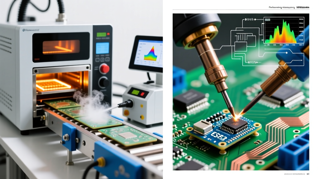
Eliminating erratic solder joints requires precise control over the thermal profile. Process engineers must move beyond generic oven recipes and tailor profiles to the specific thermal mass of the assembly.
- Ramp Rate (Room to 150°C): Maintain a ramp rate of 1.0°C to 2.0°C per second. A ramp that is too steep causes solder spattering and micro-balling; a ramp that is too slow prematurely exhausts the flux.
- Soak Zone (150°C to 217°C): Limit the soak time to 60-90 seconds. This allows the flux activators to clean the pads without boiling off completely. For heavily populated boards, extend the soak to ensure thermal equilibrium.
- Reflow / Liquidus (Above 217°C): Time Above Liquidus (TAL) should be strictly controlled between 45 and 60 seconds. Exceeding 75 seconds accelerates copper dissolution and creates brittle, grainy IMC layers that look 'mad' under microscopic cross-section analysis.
- Cooling Rate: A controlled cooling rate of 2.0°C to 4.0°C per second promotes a fine-grain microstructure, resulting in a shiny, reliable fillet. Quenching the board too fast induces thermal shock and micro-cracking.
Final Thoughts on Solder Reliability
While the search term 'real foto of mad solders' may originate from forum slang or frustrated technicians dealing with erratic reflow results, the underlying issue is a matter of rigorous process control. By understanding the metallurgical failures behind graping, HiP, and tombstoning, and by deploying advanced 3D metrology, manufacturers can ensure their assemblies meet the stringent demands of modern electronics. Always refer to the latest IPC standards and consult with your solder paste manufacturer to optimize your specific stencil and thermal profiles.