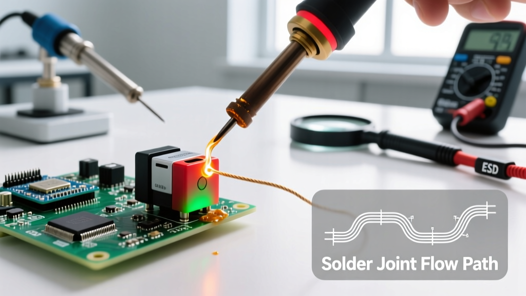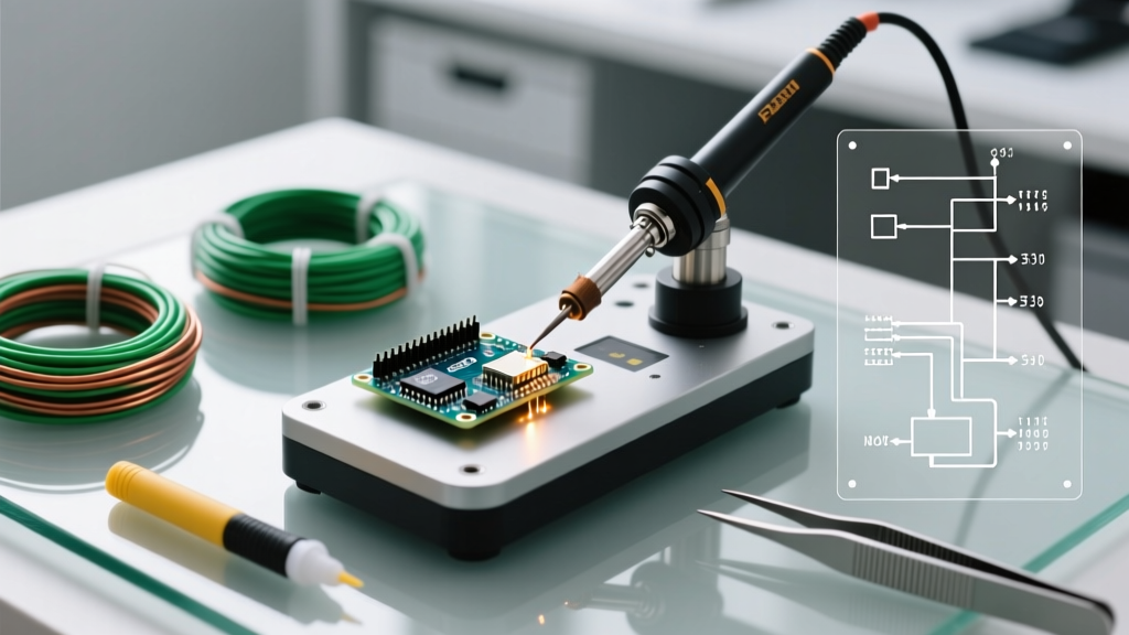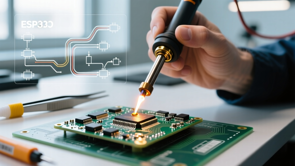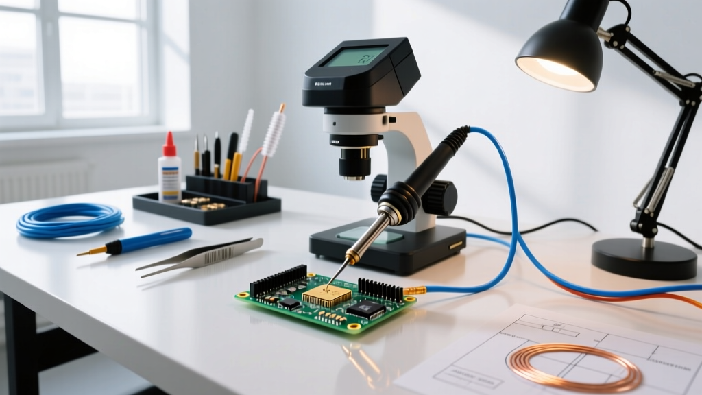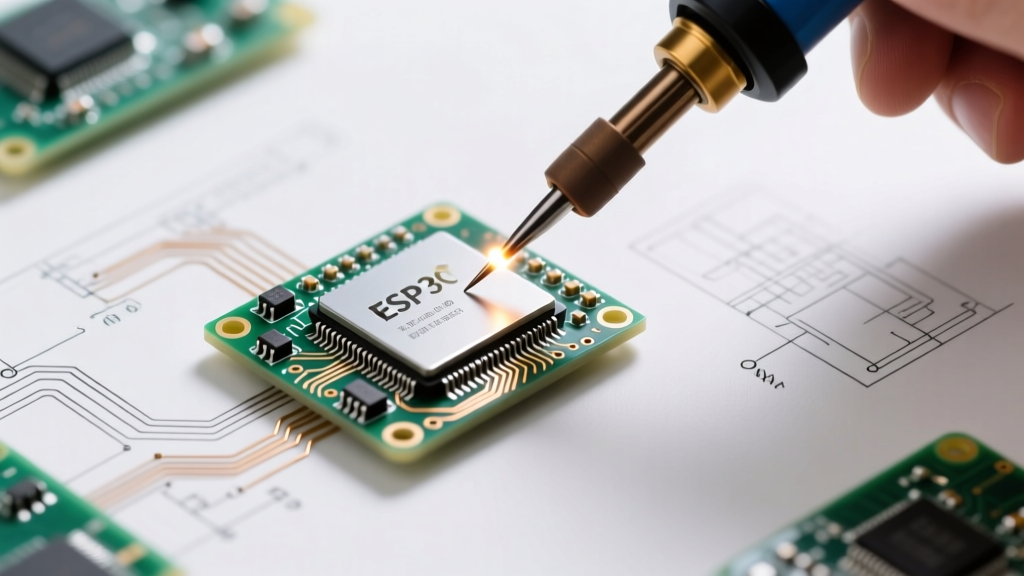

When manufacturing or repairing high-density interconnect (HDI) printed circuit boards, standard soldering irons are often too cumbersome and thermally aggressive. Enter pen soldering—the use of ultra-lightweight, pen-style micro-soldering handpieces designed for extreme precision. As we navigate the electronics manufacturing landscape of 2026, the shift toward ultra-low-profile IoT nodes, implantable medical devices, and miniaturized aerospace avionics has made pen soldering an indispensable skill and hardware category.
Unlike traditional soldering irons that rely on heavy ceramic heating elements and thick copper tips, modern pen soldering systems utilize active-tip technology. The heating element and sensor are integrated directly into the micro-tip, allowing for instantaneous thermal recovery and unmatched tactile feedback. This guide explores the critical industry applications for pen soldering, compares leading micro-pencil hardware, and outlines standard operating procedures for high-reliability PCB rework.
Core Industry Applications for Pen Soldering
The transition to micro-SMD components (such as 0201 and 01005 metric packages) requires tools that can deliver precise thermal energy without damaging adjacent traces or heat-sensitive silicon. Pen soldering dominates three major high-reliability sectors:
1. Medical Implants and Wearables
Devices like neurostimulators, continuous glucose monitors (CGMs), and modern pacemakers feature densely packed flex-PCBs and rigid-flex assemblies. These boards utilize micro-BGA and ultra-fine-pitch QFN components. Pen soldering handpieces, weighing less than 40 grams, allow technicians to maneuver around dense component forests without inducing mechanical stress on fragile flex substrates. Furthermore, the precise thermal control prevents delamination of the thin polyimide layers common in medical wearables.
2. Aerospace and Satellite Avionics
In Low Earth Orbit (LEO) satellite constellations and CubeSat avionics, every gram and millimeter counts. Aerospace PCBs often require conformal coating and operate under strict thermal cycling conditions. According to the NASA Electronic Parts and Packaging (NEPP) Program, high-reliability solder joints must avoid excessive intermetallic compound (IMC) growth, which causes brittleness. Pen soldering allows operators to limit dwell time to under two seconds per joint, minimizing IMC layer thickness while ensuring proper wetting for Sn63/Pb37 or SAC305 alloys.
3. Automotive LiDAR and Sensor Nodes
Autonomous vehicle LiDAR arrays and radar modules operate at high frequencies (77 GHz and above). The RF traces on these boards are highly sensitive to parasitic capacitance introduced by excess solder or flux residue. The pinpoint accuracy of a 0.1mm pen soldering tip ensures that solder fillets are strictly confined to the component pads, maintaining the impedance characteristics of the RF transmission lines.
Micro-Pencil Hardware Comparison Matrix
Selecting the right pen soldering station depends on your specific thermal requirements, budget, and tip ecosystem. Below is a comparison of the industry-standard micro-pencil systems utilized in professional rework labs in 2026.
| System / Handpiece | Tip Series | Max Wattage | Thermal Recovery | Approx. Cost (Station) | Best Application |
|---|---|---|---|---|---|
| JBC Nano (NT115) | C115 | 15W | < 1.5 seconds | $550 - $650 | 01005 metric, micro-BGA, flex-PCB |
| Weller WXMP | RT Micro | 40W | < 2.0 seconds | $450 - $520 | 0201 metric, fine-pitch QFP, general micro-SMD |
| Hakko FX-951 (Micro) | T12 (Micro variants) | 70W | ~ 4.0 seconds | $250 - $320 | Standard SMD, larger ground planes, budget labs |
For pure miniaturization, the JBC Tools Nano system remains the undisputed king. The C115 tip series offers cartridge-style replacements where the heater, sensor, and tip are a single unit, eliminating thermal transfer lag. However, for labs that need a balance between micro-soldering and slightly larger thermal mass components (like 0402 or small QFNs), the Weller WXMP provides a more versatile ergonomic grip and a broader RT micro tip selection.
Thermal Profiling and Dwell Time Constraints
Industry Insight: In high-reliability Class 3 assemblies, the goal of pen soldering is not just to melt the solder, but to achieve a specific thermal profile within a constrained time window. Exceeding a 3-second dwell time on micro-pads risks pad lifting and substrate degradation.
When pen soldering lead-free SAC305 (melting point 217°C), the iron temperature should typically be set between 320°C and 350°C. While this seems high, the micro-mass of the pen tip means the actual temperature at the joint interface drops rapidly upon contact. A high starting temperature ensures the solder reflows within 1.5 to 2.5 seconds. If the iron is set too low (e.g., 280°C), the operator will be forced to hold the tip on the pad for 5+ seconds to achieve reflow, which transfers excessive total thermal energy (Joules) into the PCB, causing internal via barrel cracking or pad delamination.
Navigating IPC Standards and Failure Modes
All industrial pen soldering must comply with the IPC J-STD-001 standard for soldered electrical and electronic assemblies. For aerospace and medical devices, technicians must adhere to Class 3 requirements, which demand maximum wetting, specific fillet geometries, and zero tolerance for solder balls or bridging.
Common Pen Soldering Failure Modes
- Tombstoning: Caused by asymmetric heating. If the pen tip contacts one pad before the other, the solder on the heated pad melts first, and the surface tension pulls the component upright. Solution: Use a chisel or micro-knife tip to bridge both pads and the component termination simultaneously.
- Flux Spatter and Dendritic Growth: Micro-tips require highly concentrated, low-solids no-clean flux. Applying too much liquid flux causes violent outgassing (spatter) when the pen tip makes contact, leaving residue that can lead to electrochemical migration (dendrites) in humid environments.
- Tip Oxidation: Because pen soldering tips have incredibly small surface areas, a single instance of leaving the iron in its holder without a solder cap will oxidize the tip within minutes, ruining its wettability. Always tin the micro-tip with a generous blob of SAC305 before docking.
Step-by-Step: Pen Soldering a 0201 Metric Component
The 0201 metric component (0.6mm x 0.3mm) is a benchmark for pen soldering proficiency. Follow this exact procedure for high-yield rework:
- Preparation: Clean the PCB pads with 99% isopropyl alcohol (IPA). Inspect under a 20x stereomicroscope to ensure no oxidation or conformal coating residue remains on the pads.
- Flux Application: Apply a microscopic dot of tacky no-clean flux (e.g., Chip Quik NC191 or Indium5.2LT) using a 0.5mm dispensing needle. The flux should only cover the pads, not the surrounding solder mask.
- Pre-Tinning: Using your pen soldering iron (set to 330°C with a 0.2mm micro-chisel tip), lightly pre-tin one of the two pads. The solder fillet should be no higher than 0.1mm.
- Component Placement: Using vacuum pickup tweezers or fine-point ceramic tweezers, place the 0201 component onto the pads.
- First Joint: Gently press the pen tip against the pre-tinned pad and the component termination simultaneously. Hold for exactly 1.0 to 1.5 seconds until the solder flows. Remove the iron, then release the tweezers.
- Second Joint: Apply a microscopic amount of solder wire (0.25mm diameter) to the opposite pad. Touch the pen tip to the pad and termination. Capillary action and the flux will pull the solder into a perfect concave fillet within 1.5 seconds.
- Inspection: Verify under the microscope that both fillets exhibit a smooth, shiny, concave shape with visible wetting angles, fully compliant with IPC-A-610 Class 3 visual requirements.
Conclusion
Pen soldering is no longer a niche technique; it is a fundamental requirement for modern electronics manufacturing and high-reliability rework. By investing in active-tip micro-pencil systems like the JBC Nano or Weller WXMP, and strictly adhering to thermal dwell time limits and IPC J-STD-001 guidelines, production facilities can achieve near-perfect yields on the most densely packed HDI assemblies of 2026 and beyond. Mastery of the pen soldering technique bridges the gap between theoretical PCB design and functional, field-ready microelectronics.