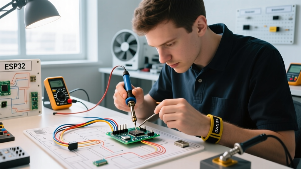

PCB to PCB soldering—whether stacking daughterboards, creating edge-to-edge bridges, or wire-harnessing multiple modules—presents unique thermal and chemical hazards compared to standard component-to-board assembly. When joining two printed circuit boards, the combined thermal mass and complex ground planes can lead to prolonged heating, increasing the risk of delamination, toxic flux outgassing, and thermal burns. This guide outlines the critical safety best practices for PCB to PCB soldering in 2026, ensuring both operator protection and IPC-A-610 Class 3 compliant joints.
Thermal Management: Overcoming Dual-Board Thermal Mass
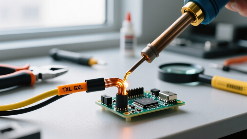
When soldering a pin from a top PCB through a via into a bottom PCB, the copper ground planes act as massive heat sinks. Using a standard 40W iron results in 'cold pushing,' where the operator holds the iron in place for 10+ seconds waiting for the solder to flow. This causes severe flux degradation, toxic smoke spikes, and irreversible board damage.
Equipment Selection for High-Mass Joints
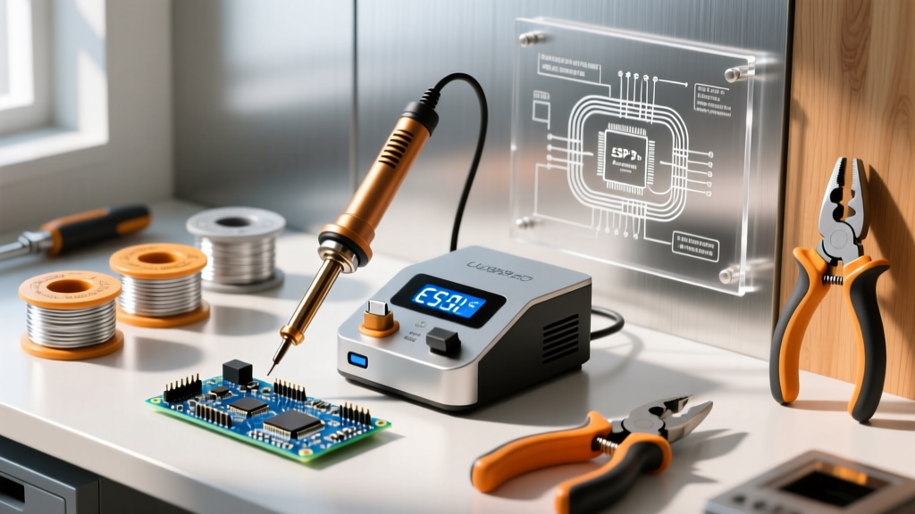
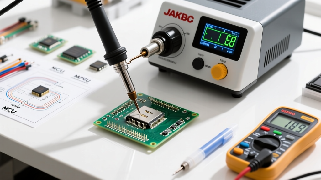
You need active-tip, high-wattage stations to maintain thermal equilibrium. The Weller WE1010NA ($115, 70W) is the baseline for hobbyists, but for multi-layer PCB-to-PCB stacks, the JBC CD-2BQE ($650, 130W) or Hakko FX-951 ($295, 70W with rapid thermal recovery) is strictly required. Set your tip temperature to 350°C (662°F) for SAC305 lead-free alloy. The high wattage ensures the tip recovers its temperature within 2 seconds of touching the dual thermal mass, limiting contact time to the safe 2-3 second window mandated by industry standards.
Fume Extraction and Flux Toxicity
PCB to PCB soldering often requires copious amounts of flux to ensure capillary action pulls the solder through deep, stacked vias. This generates significant colophony (rosin) smoke. According to the UK Health and Safety Executive's HSG255 guidelines on rosin flux, repeated inhalation of rosin-based flux fumes can cause occupational asthma and severe respiratory sensitization.
Source-Capture Extraction Systems
Never rely on passive desk fans, which merely blow toxic aliphatic aldehydes into your breathing zone. You need HEPA and activated carbon source-capture extraction.
- Hobbyist Tier: The Hakko FA-400 ($65) provides basic localized particulate capture but lacks the carbon mass to filter volatile organic compounds (VOCs).
- Professional Tier: The BOFA AD375 ($1,400) or Metcal BVX-200 ($850) utilize deep-bed activated carbon to neutralize toxic VOCs released during high-mass soldering, ensuring a safe breathing environment.
Electrostatic Discharge (ESD) and Grounding Protocols
Joining two active PCBs often means handling exposed microcontrollers, FPGAs, and sensitive MOSFETs. A human body can easily accumulate 3,000V to 5,000V of static charge in a dry environment. As outlined by the ESD Association (ESDA), an uncontrolled discharge will instantly gate-rupture sensitive silicon, leading to latent field failures.
CRITICAL GROUNDING RULE: Ensure your soldering station tip, ESD mat, and wrist strap are all tied to the exact same common point ground. A potential difference between the iron tip and the PCB ground plane will cause a discharge directly through the board's components.
Implement a verified grounding loop using a Desco 19233 continuous monitor wrist strap ($145) connected to a 3M 8214 static dissipative mat ($85). The mat must have a resistance to ground (Rg) between 1.0 x 10^6 and 1.0 x 10^9 ohms. This 'slow bleed' resistance prevents a sudden, destructive discharge while safely draining static buildup.
Solder Alloy and Flux Safety Matrix for PCB Stacking
Choosing the right chemistry minimizes toxic exposure and ensures reliable intermetallic compound (IMC) formation across dual boards.
| Alloy / Flux Type | Melting Point | Safety & Handling Profile | Best Use Case |
|---|---|---|---|
| SAC305 (Sn96.5/Ag3.0/Cu0.5) + ROL0 | 217°C - 220°C | Lead-free; ROL0 is low-activity, minimizing corrosive residues and toxic fumes. | Standard commercial PCB-to-PCB stacking. |
| Sn63/Pb37 + RMA | 183°C | Contains Lead (Pb). Requires strict hygiene, dedicated tools, and hazardous waste disposal. | Legacy repairs, aerospace (where exempt). |
| Sn42/Bi57.6/Ag0.4 + No-Clean | 138°C - 145°C | Ultra-low temp. Drastically reduces thermal burn risk and flux outgassing. | Heat-sensitive RF boards and flex-PCB bridges. |
Mechanical Fixturing: Preventing Physical and Thermal Trauma
Holding two PCBs by hand while applying a 350°C iron is a recipe for catastrophic failure. Micro-movements during the cooling phase (solidification) cause disturbed joints, characterized by a dull, grainy appearance and internal micro-fractures. More importantly, slipping while handling stacked boards leads to severe operator burns or short circuits on live test setups.
Recommended Fixturing Gear
Use articulating third-hands to lock boards in place. The QuadHands Workbench ($65) with flexible magnetic arms or a heavy-duty PanaVise 201 ($45) modified with ESD-safe silicone jaws ($15) will lock both PCBs in perfect Z-axis alignment. This allows the operator to keep both hands free—one for the iron, one for the solder wire—ensuring precise feed rates and immediate withdrawal once the meniscus forms.
Troubleshooting Common PCB-to-PCB Failure Modes
Even with perfect safety protocols, the physics of dual-board soldering can cause distinct failure modes. Here is how to identify and safely resolve them:
- Solder Wicking and Starved Joints: When stacking, capillary action pulls solder away from the top pad into the via barrel. Resolution: Use a slightly larger bevel tip (e.g., JBC C115-112) and apply additional no-clean flux (Amtech NC-559-V2-TF) to the top pad to break surface tension and retain the solder fillet.
- Thermal Delamination: The FR4 glass transition temperature (Tg) is typically 130°C-170°C. Prolonged heating causes the epoxy to expand and separate from the copper, creating a 'measling' effect. Resolution: Pre-heat the bottom PCB using an 853D Preheater ($120) set to 100°C. This reduces the thermal delta, allowing a lower iron tip temp (320°C) and faster flow times.
- Electrochemical Migration (Dendrites): Flux trapped between tightly stacked PCBs can absorb ambient moisture, creating conductive dendrite growth that shorts adjacent vias. Resolution: Always clean dual-board assemblies with 99% Isopropyl Alcohol (IPA) and an ESD-safe hog-hair brush, followed by a low-pressure air blowout to displace trapped liquid.
Workspace Hygiene and Post-Soldering Cleanup
According to Stanford University's Environmental Health & Safety soldering protocols, lead and heavy metal residues from solder alloys and flux activators pose severe ingestion risks if proper hygiene is ignored. Never eat, drink, or apply cosmetics at the soldering bench.
After completing a PCB-to-PCB integration, wash hands with cold water and soap (cold water keeps skin pores closed, preventing lead dust absorption before washing). Wipe down your ESD mat daily with an ESD-safe cleaner like Desco Reztore ($18) to maintain the mat's dissipative properties and remove microscopic solder splatter that could later puncture delicate flex cables.
A Final Warning on Integrated Power Sources
WARNING: When performing PCB-to-PCB soldering on devices with integrated lithium-polymer (LiPo) batteries, always physically disconnect or desolder the battery leads first. A stray iron slip or solder splash across adjacent power rails can cause an unrecoverable thermal runaway event. Treat all multi-board assemblies as live until verified with a multimeter.
By respecting the thermal mass, managing chemical exposure, and enforcing strict ESD and mechanical protocols, you ensure that your PCB to PCB soldering projects are both exceptionally reliable and entirely safe for the operator.