
The 2026 Expert Roundup: Elevating Your PCB Soldering Technique
Soldering to a PCB is often introduced as a simple hobbyist skill, but bridging the gap between a functional prototype and a Class 3 aerospace-grade assembly requires a deep understanding of metallurgy, thermodynamics, and fluid dynamics. As surface-mount components shrink to 0201 and 01005 imperial sizes, and high-density interconnect (HDI) boards become the standard in 2026, the margin for error has virtually disappeared. To provide the most authoritative guide on soldering to a PCB, we have synthesized insights from IPC-certified trainers, senior hardware engineers, and manufacturing leads. This expert roundup breaks down the exact methodologies, tools, and failure-mode preventions used in modern electronics manufacturing.
1. The Metallurgist: Alloy and Flux Selection for Modern Boards
The foundation of any reliable solder joint lies in the chemical composition of the alloy and the flux vehicle. According to IPC J-STD-001 requirements for soldered electrical and electronic assemblies, matching your consumables to the thermal mass of the board is non-negotiable.
Leaded (Sn63Pb37) vs. Lead-Free (SAC305)
While the consumer market has largely transitioned to lead-free alloys, many prototyping, aerospace, and medical labs still rely on Sn63Pb37 (63% Tin, 37% Lead). This eutectic alloy melts at a precise 183°C (361°F) and transitions from liquid to solid instantly, preventing the micro-cracking associated with the plastic state of non-eutectic mixes. However, for commercial production in 2026, SAC305 (96.5% Sn, 3.0% Ag, 0.5% Cu) remains the dominant lead-free standard. SAC305 melts between 217°C and 220°C, requiring higher iron temperatures (typically 350°C to 380°C) and exposing the PCB substrate to greater thermal stress.
Flux Chemistry: The Unsung Hero
"The biggest mistake I see engineers make is treating flux as an afterthought," notes a senior metallurgist from a leading EMS provider. Flux removes oxidation from the copper pads and component leads, allowing the solder to wet the surface. For high-reliability PCB soldering, experts recommend ROL0 (Rosin, Low activity, 0% halides) fluxes, such as Kester 186. These are benign if left uncleaned. Conversely, water-soluble (OA) fluxes like Amtech NC-559-V2-TF offer superior wetting for challenging finishes like ENIG or OSP but must be aggressively cleaned with heated deionized water post-soldering to prevent catastrophic electrochemical migration (dendritic growth) over time.
2. The Thermal Engineer: Heat Transfer and Tip Geometry
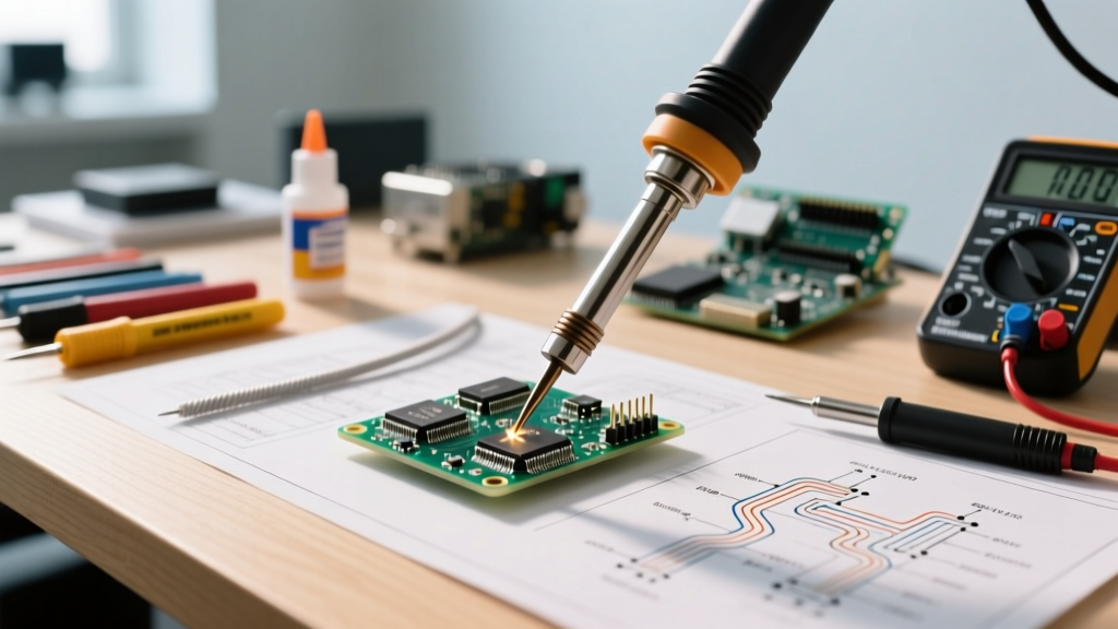
When soldering to a PCB, the goal is to transfer heat to the pad and the component lead simultaneously, reaching the alloy's liquidus temperature in under three seconds. The choice of soldering iron and tip geometry dictates this thermal transfer.
Active Cartridge vs. Passive Ceramic Heaters
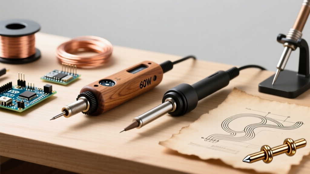
In 2026, active cartridge systems are the undisputed standard for professional PCB work. Stations like the Pace TF-2700 with TD-200 AccuDrive or the Hakko FX-951 utilize tips where the heating element and sensor are integrated directly into the copper core. This eliminates the thermal lag found in older passive ceramic heaters (like the classic Hakko 936), allowing the iron to instantly dump wattage into large ground planes without dropping below the setpoint.
Tip Geometry Matrix
Using the wrong tip shape is the primary cause of cold joints and pad delamination. Below is the expert consensus on tip selection:
| Tip Geometry | Best Application | Thermal Transfer Efficiency | Expert Warning |
|---|---|---|---|
| Chisel (D-Shaped) | Through-hole, large 0805+ SMD, tinning wires | Excellent (Maximum surface contact) | Can bridge fine-pitch IC pins if too wide. |
| Hoof / Micro-Hoof | Drag soldering TQFP/QFP, clearing solder bridges | Very High (Holds a solder wave) | Requires precise angle control; prone to oxidation if tinned poorly. |
| Conical (Pointed) | Micro-soldering, 0201 components, tight clearance | Poor (Minimal surface area contact) | Avoid for general PCB pads; causes prolonged dwell times and pad lift. |
| Knife (K-Tip) | Vertical drag soldering, cutting small solder bridges | High (Edge contact) | Wears down quickly on abrasive lead-free finishes. |
3. The Reliability Inspector: IPC-A-610 Defect Prevention
To understand what constitutes a perfect joint, we look to the NASA Workmanship Training Program and the IPC-A-610 standard, which categorizes solder joints into Target (Ideal), Acceptable, and Defect. When soldering to a PCB for Class 3 (high-performance, life-support, or aerospace) applications, the requirements are stringent.
"A shiny joint does not necessarily mean a good joint, especially with lead-free SAC alloys which naturally dry dull and grainy. Inspectors must look at the wetting angle and the fillet profile, not just the reflectivity." — IPC-Certified Master Specialist
Common Failure Modes and Prevention
- Tombstoning (Drawbridging): Common on 0402 and 0201 passives. Occurs when one pad heats faster than the other, causing the surface tension of the molten solder to pull the component upright. Prevention: Ensure symmetrical thermal relief traces on both pads and apply heat evenly to the pad, not the component body.
- Solder Wicking (Solder Theft): Solder flows up the component lead away from the PCB pad, leaving a starved joint. Prevention: Apply the iron to the pad first, then introduce the solder wire to the pad-lead intersection. Never feed solder directly onto the iron tip and attempt to "paint" it onto the joint.
- Pad Delamination (Lifted Lands): The copper pad separates from the FR-4 substrate. This is a catastrophic failure caused by exceeding the glass transition temperature (Tg) of the laminate for too long. Prevention: Limit dwell time to under 3 seconds per joint. If a joint requires 5+ seconds of continuous heat, your iron temperature is too low or your tip thermal mass is insufficient.
4. The Rework Specialist: Desoldering Without Board Damage
Expertise in soldering to a PCB is incomplete without mastering desoldering. In modern rework, minimizing thermal cycling is critical to preserving the integrity of the plated through-holes (PTH) and internal vias.
Solder Wick vs. Vacuum Extraction
For clearing surface mount pads, high-quality desoldering braid is mandatory. Experts recommend Chemtronics Soder-Wick (specifically the #3 Rosin or #4 Blue labels) in widths of 2.0mm to 3.5mm. The copper braid acts as a thermal bridge, pulling heat and molten solder away from the pad via capillary action. Pro-Tip: Never drag dry braid across a pad. Always pre-tin the braid slightly or add a small amount of fresh leaded solder to the joint first; this lowers the melting point of the existing lead-free solder (a process known as cross-alloying) and drastically reduces the heat required for removal.
For through-hole components, vacuum desoldering guns like the Hakko FR-301 or the Edsyn SOLDAPULLT DS01-LS are essential. These tools feature PTFE-coated nozzles that resist solder buildup and allow for one-handed operation, freeing your other hand to stabilize the PCB and extract the component the moment the solder liquefies.
Expert Troubleshooting Matrix
When your soldering to a PCB yields inconsistent results, use this diagnostic matrix to identify the root cause:
| Observed Defect | Probable Root Cause | Expert Corrective Action |
|---|---|---|
| Solder balls up and refuses to wet the pad | Severe oxidation on pad or component; flux exhaustion. | Clean pad with IPA and fiberglass pen. Apply fresh liquid flux. Lower iron temp to prevent flux burn-off. |
| Joint looks cracked, dull, and disturbed | Movement during the solidification phase (non-eutectic plastic state). | Hold the component completely still until the solder loses its liquid sheen. Use a PCB vise or helping hands. |
| Excessive flux spattering and popping | Iron temperature too high; boiling the flux solvents instantly. | Drop station temperature by 20°C. Switch to a lower-activity flux or a flux with a higher boiling point solvent. |
| Solder flows onto the solder mask (solder balls) | Lack of solder mask defined (SMD) pads; inadequate flux. | Use a flux pen to define the wetting boundary. Ensure the iron tip is clean to prevent random solder transfer. |
Final Takeaways for 2026
Mastering the art of soldering to a PCB requires moving beyond basic tutorials and adopting an engineering mindset. By selecting the correct alloy and flux chemistry for your specific board finish, utilizing active-cartridge irons with appropriate chisel or hoof geometries, and strictly adhering to IPC thermal dwell limits, you can achieve manufacturing-grade reliability on your workbench. Whether you are assembling a custom microcontroller array or repairing a multi-layer telecommunications board, the principles of thermodynamics and metallurgy remain your most valuable tools.
For further reading on advanced assembly standards, consult the latest revisions of CircuitNet's expert manufacturing forums and the IPC workmanship manuals to keep your skills aligned with current industry benchmarks.