
The Metallurgy of Solderability: Beyond the Melt
When electronics engineers and DIYers discuss solderability, they are rarely talking about the mere melting of tin-lead or SAC305 alloys. True solderability is a metallurgical phenomenon defined by the wetting angle (theta) and the rapid formation of an Intermetallic Compound (IMC) layer. A wetting angle of less than 90 degrees indicates proper wetting, while anything above 90 degrees signals dewetting or non-wetting. For a reliable electrical and mechanical bond, the molten solder must dissolve the surface finish and react with the base metal—typically copper—to form a Cu6Sn5 (eta phase) IMC layer, followed by a slower-growing Cu3Sn (epsilon phase) layer.
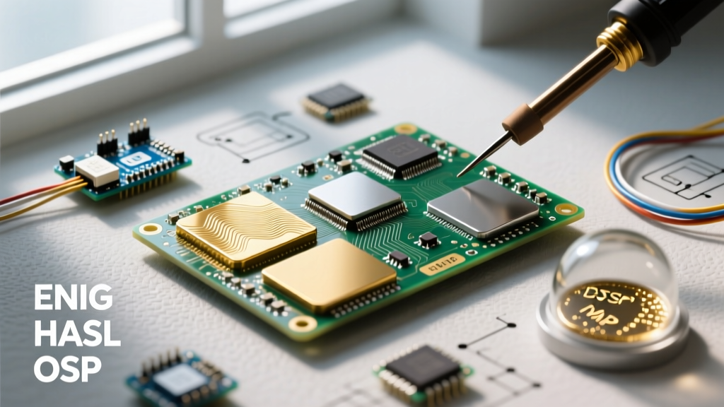
Choosing the right PCB surface finish is the most critical purchasing decision for ensuring long-term solderability. In 2026, with the miniaturization of components down to 0.35mm pitch BGAs and the volatility of precious metal markets, understanding how Hot Air Solder Leveling (HASL), Electroless Nickel Immersion Gold (ENIG), and Organic Solderability Preservatives (OSP) behave under the iron or in the reflow oven is essential. Below, we compare these three dominant finishes across solderability metrics, shelf life, and flux compatibility.
Surface Finish Comparison Matrix (2026 Data)
| Metric | Lead-Free HASL | ENIG | OSP |
|---|---|---|---|
| Base Solderability | Good (Uneven topography) | Excellent (Ultra-flat) | Very Good (Degrades fast) |
| IMC Formation | Cu6Sn5 (Pre-tinned) | Ni3Sn4 (Nickel-Tin) | Cu6Sn5 (Direct to Copper) |
| Shelf Life (Sealed) | 12 - 18 Months | 12 - 24 Months | 6 Months (Strict) |
| Multi-Reflow Survival | Excellent | Excellent | Poor (Oxidizes after 1st pass) |
| Avg. Cost Adder (10x10cm) | ~$0.00 (Base) | ~$18.00 - $25.00 | ~$1.00 - $3.00 |
| Ideal Component Pitch | > 0.8mm (Thru-hole/Large SMD) | < 0.5mm (BGA, QFN, Edge Connectors) | < 0.5mm (Fine-pitch SMD) |
Deep Dive: HASL (The Budget Workhorse)
HASL involves dipping the bare copper PCB into a bath of molten lead-free solder (typically Sn-0.7Cu, melting at 227°C) and then using hot air knives to blow off the excess.
Solderability Realities
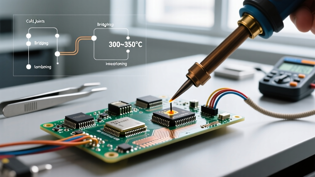
Because the board is already coated in solder, initial wetting is nearly instantaneous. The flux in your solder wire simply needs to clean minor surface oxidation. However, the meniscus effect causes the solder to pool at the edges of the pads, creating a rounded, uneven surface. If you are hand-soldering a 0.5mm pitch TQFP or a 0.4mm BGA, this uneven topography will cause bridging and tombstoning. Furthermore, the high thermal shock of the HASL process can stress vias and degrade the FR4 laminate if the board has a high layer count.
Failure Mode Alert: When hand-soldering HASL boards that have exceeded their 12-month shelf life, the tin-copper surface develops a stubborn SnO2 oxide layer. Standard RMA (Rosin Mildly Activated) flux will fail to break this down. You must upgrade to a water-soluble or high-activity no-clean flux (e.g., Kester 951) to achieve proper wetting.
Deep Dive: ENIG (The Premium Standard)
ENIG utilizes a two-step chemical deposition process: an electroless nickel plating (150-200 microinches) followed by a thin immersion gold flash (1-3 microinches).
The Gold Dissolution Myth
A common misconception among junior engineers is that the gold participates in the solder joint. In reality, the gold layer exists solely to protect the underlying nickel from oxidation during storage. Upon contact with molten SAC305 solder, the gold dissolves into the tin matrix in milliseconds. The actual solder joint forms between the tin and the nickel, creating a Ni3Sn4 IMC layer. This nickel-tin IMC grows much slower than copper-tin IMCs, making ENIG joints highly resistant to thermal fatigue and ideal for harsh environments.
2026 Market Context & Black Pad Syndrome
Due to sustained high gold commodity prices through 2025 and 2026, ENIG costs have risen by roughly 15% compared to a decade ago, pushing many hobbyists toward OSP. However, ENIG remains mandatory for gold-finger edge connectors and wire-bonding pads. The primary solderability risk with ENIG is Black Pad Syndrome—a hyper-corrosion of the nickel layer caused by aggressive galvanic baths during manufacturing. This results in a brittle, phosphorus-rich nickel layer that fractures under minor mechanical stress. Always source ENIG boards from fabs that strictly adhere to IPC-4552B standards to ensure the gold thickness does not exceed 3 microinches, which exacerbates gold embrittlement.
Deep Dive: OSP (The Ultra-Flat Specialist)
OSP is a water-based, organic chemical layer (typically a benzimidazole or azole compound) that bonds to the bare copper, preventing oxidation. It is incredibly thin (0.2 to 0.5 microns) and leaves the pad perfectly flat.
Solderability Challenges
OSP provides phenomenal solderability if the board is fresh. The organic layer vaporizes instantly upon contact with heat and flux. However, OSP is highly unforgiving regarding shelf life and handling. Human skin oils and ambient humidity will degrade the azole layer within hours of opening the vacuum-sealed packaging. Furthermore, OSP does not survive multiple reflow cycles well. After the first pass through the reflow oven, the exposed copper rapidly oxidizes, making secondary hand-soldering or rework exceptionally difficult without aggressive mechanical abrasion.
For a comprehensive breakdown of how OSP interacts with modern no-clean fluxes, refer to the Seeed Studio Surface Finish Breakdown, which highlights the necessity of nitrogen-enriched reflow environments for high-yield OSP assembly.
The Flux Pairing Framework: Matching Chemistry to Finish
Solderability is a two-part system: the surface finish and the flux chemistry. Using the wrong flux on a specific finish is the leading cause of cold joints and dewetting in DIY and small-batch manufacturing. Below is the definitive 2026 flux pairing guide:
- For ENIG: Use a Mildly Activated Rosin (RMA) or a standard No-Clean tacky flux. Recommendation: Amtech NC-559-V2-TF. The gold dissolves effortlessly; aggressive halide-based fluxes are unnecessary and can trap corrosive residues under fine-pitch BGAs where cleaning is impossible.
- For OSP: Use a high-activity, high-solids flux. The flux must penetrate and break down the organic azole layer before the copper underneath can oxidize from the heat. Recommendation: Kester 951 (Water-Soluble) or Chip Quik TS391-T50. If using a liquid flux pen, apply it before the iron touches the pad to prevent the OSP from baking into a hard, non-wettable carbon shell.
- For HASL: Standard No-Clean fluxes work perfectly. Recommendation: Chip Quik NC191 or standard 63/37 Rosin-Core wire. The surface is already tinned, so the flux only needs to act as a mild deoxidizer.
Validating Solderability: The IPC Dip-and-Look Test
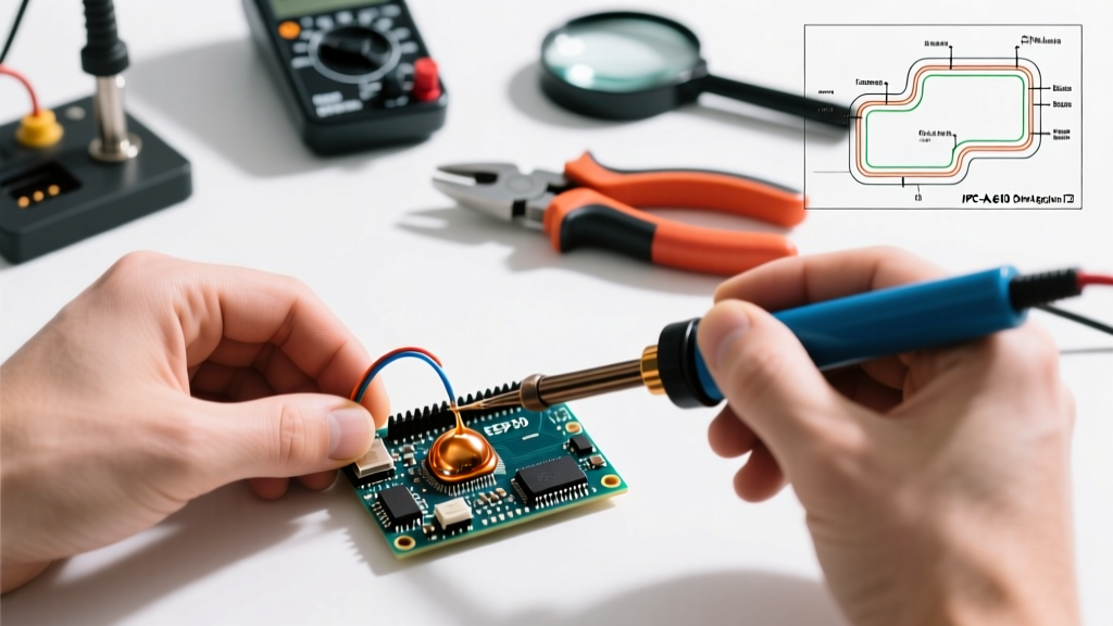
If you are purchasing surplus PCBs or evaluating a new fabrication house, do not rely on visual inspection. Oxidation on ENIG and HASL is often invisible to the naked eye. Instead, perform a simplified IPC J-STD-003B Dip-and-Look test.
- Set a static-safe solder pot to 245°C ± 5°C (for lead-free SAC305 evaluation).
- Dip the PCB edge or a test coupon into a mild RMA flux.
- Immerse the board into the molten solder for exactly 5 seconds.
- Extract and inspect under 10x magnification.
Pass Criteria: The pads should exhibit a smooth, bright, continuous solder coating with a wetting angle of less than 90 degrees. Pinholes, dewetted areas (where solder pulls back into droplets), or non-wetted copper spots indicate a compromised surface finish or expired shelf life. For further reading on the advantages and limitations of these finishes in high-reliability aerospace applications, consult Altium's PCB Surface Finish Guide.
Final Buyer's Verdict
If your design features 0.4mm pitch BGAs, RF impedance-controlled traces, or edge connectors, absorb the 2026 premium and order ENIG. If you are building high-volume, single-sided consumer IoT devices with fine-pitch passives and have a strict BOM/PCB budget, OSP is your best choice—provided you assemble them within 30 days of delivery. For thru-hole connectors, heavy power planes, and general hobbyist prototyping where pad flatness is irrelevant, HASL remains the undisputed, cost-effective champion of immediate solderability.