
The Evolution of Board-Level Repair in 2026
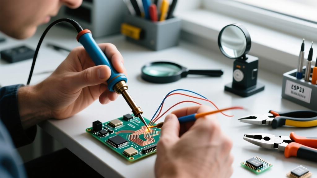
As logic board architectures shrink to accommodate high-performance silicon like the Apple M4 and Snapdragon 8 Gen 3, the discipline of micro soldering has transitioned from a niche hobby to a mission-critical engineering skill. Modern micro soldering routinely involves manipulating 01005 imperial (0402 metric) passive components, executing 0.01mm jumper trace repairs, and performing blind BGA (Ball Grid Array) rework. To understand the current state of the art, we convened a roundup of three industry veterans: Marcus Thorne (Lead Data Recovery Engineer), Elena Rostova (Independent Board-Level Repair Specialist), and David Chen (Aerospace Avionics Technician). Their collective insights reveal the exact tools, thermal profiles, and consumables required to meet strict IPC J-STD-001 reliability standards in 2026.
Optics and Illumination: The Foundation of Micro Rework
You cannot solder what you cannot see. The consensus among our experts is that investing in premium optics yields a higher ROI than any soldering station. Elena Rostova emphasizes the necessity of a true stereo zoom microscope with a continuous magnification range of 7x to 45x.
'In 2026, relying on a digital USB microscope for actual rework is a recipe for pad cratering. You need true optical depth perception and zero latency. I use the AmScope SM-4TZ (approx. $450) with a 0.5x Barlow lens to increase my working distance to 90mm, which is critical when maneuvering hot air nozzles and micro-scalpels.' — Elena Rostova
Lighting Configurations
- Dual Gooseneck LED: Essential for raking light to inspect solder joint fillets and detect micro-fractures in MLCCs.
- Polarizing Filters: Marcus Thorne insists on polarizing both the light source and the objective lens. 'Flux residue creates intense specular glare under high-intensity LEDs. Cross-polarization cuts the glare, allowing you to verify wetting on 0201 pads without washing the board mid-process.'
Thermal Profiling: Soldering Stations & Hot Air
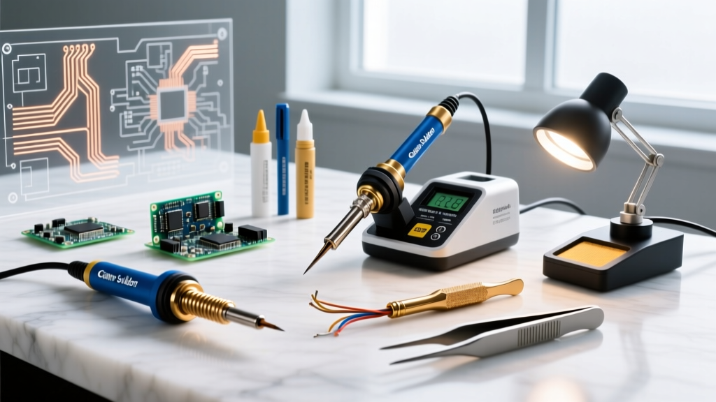
Thermal mass management is the defining factor in micro soldering success. The days of using a generic 60W ceramic heater are over; modern ground planes on multi-layer PCBs act as massive heat sinks, requiring stations with rapid thermal recovery.
Expert Station Comparison Matrix
| Brand & Model | Approx. Price (2026) | Best Use Case | Expert Verdict |
|---|---|---|---|
| JBC CD-2BQE | $650 - $720 | Precision SMD, 01005 passives, jumper wires | Unmatched recovery time. The C115-112 spoon tip holds micro-scavenging capability without lifting adjacent pads. |
| Quick 861DW | $350 - $380 | BGA rework, shield removal, connector desoldering | Industry standard for hot air. Programmable profiles prevent thermal shock to surrounding NAND chips. |
| Hakko FX-951 | $320 - $350 | General through-hole, larger SMD, budget setups | Reliable workhorse, but the T15 tip series lacks the micro-geometry required for sub-0402 rework. |
David Chen notes that tip selection is just as critical as the station. 'For trace repair, I use the JBC C115-106 (knife) at 320°C. The knife edge allows you to drag a 0.1mm bead of 63/37 SnPb solder along a scraped trace without bridging to the adjacent ground plane.'
Consumables: Flux, Wire, and Masking
The physical materials used in micro soldering dictate the long-term reliability of the repair. Our panel universally rejects cheap, unbranded fluxes from online marketplaces due to inconsistent activation temperatures and corrosive halide content.
The 2026 Consumables Checklist
- Flux: Amtech NC-559-V2-TF (approx. $45 per 10cc syringe). This no-clean, lead-free compatible flux offers a high-tack viscosity that holds 01005 components in place before reflow, while leaving a benign, non-conductive residue that prevents parasitic capacitance in RF circuits.
- Jumper Wire: 0.01mm (10-micron) polyurethane-enameled copper wire. Elena warns against mechanical stripping: 'Never use a wire stripper on 0.01mm wire; you will shear the core. Strip the enamel chemically with a specialized dip, or thermally by applying flux and touching it with a 350°C iron for 1.5 seconds.'
- Solder Mask: UV-curable solder resist (e.g., Senyu). Used to encapsulate jumper wires and prevent short circuits against metal RF shields.
Edge Cases: Avoiding MLCC Fractures and Pad Cratering
Micro soldering is fraught with hidden failure modes. The most catastrophic is the fracturing of Multi-Layer Ceramic Capacitors (MLCCs) due to thermal shock. When a 120°C board is suddenly hit with 380°C hot air, the dielectric layers inside the capacitor crack, leading to dead shorts that are nearly impossible to diagnose without thermal imaging.
Expert Protocol for Thermal Ramping
To mitigate this, Marcus Thorne mandates a strict pre-heating protocol: 'Always use a PCB pre-heater set to 100°C, or manually ramp your hot air station. Start at 120°C with high airflow (40L/min) for 45 seconds to outgas moisture and equalize the board temperature. Only then do you switch to your reflow profile of 360°C-380°C. This keeps the thermal gradient below 3°C per second, which is the threshold for MLCC dielectric failure.'
Another common edge case is pad cratering—where the copper pad tears away from the underlying fiberglass substrate. This usually occurs when a technician applies lateral mechanical force with tweezers while the solder is in a semi-solid (pasty) phase. The fix requires scraping the trace back to healthy copper, tinning the exposed trace, and anchoring a jumper wire using UV solder mask for structural support.
Expert FAQ: Micro Soldering Nuances
Is lead-free solder mandatory for board-level repair?
No. While consumer electronics are manufactured with SAC305 (lead-free) to comply with RoHS, the repair industry predominantly uses 63/37 Tin-Lead (SnPb) eutectic solder. SnPb melts at a lower temperature (183°C vs 217°C), reducing thermal stress on the PCB. Mixing SnPb with the factory lead-free solder creates a mixed-metal joint with a lower melting point and excellent wetting characteristics, which is highly reliable for localized repairs.
How do you clean flux residue from under a BGA chip?
David Chen advises against aggressive scrubbing. 'After a BGA reball and reflow, use a low-pressure aerosol flux remover (like MG Chemicals 413C) with a soft hake brush. Capillary action will wick the solvent and dissolved flux out from under the chip. Follow up with a 60°C bake in a convection oven for 20 minutes to evaporate trapped moisture.'
What is the minimum trace width for a reliable jumper?
For standard 5V to 12V logic lines, a 0.01mm enameled copper wire is sufficient, capable of carrying up to 0.5A continuously. However, for power rails (e.g., VDD_MAIN or battery lines drawing 3A+), you must use 0.1mm or 0.2mm bare copper wire, soldered across multiple vias to distribute the current load and prevent localized thermal runaway.