
The Metallurgy of a Reliable Soldered Joint
A high-reliability soldered joint is not merely an electrical bridge or a mechanical glue; it is a complex metallurgical alloy formed at the boundary of the base metal and the solder. When molten solder contacts a copper pad, an Intermetallic Compound (IMC) layer forms instantly. For standard Tin-Lead (Sn63/Pb37) and Lead-Free (SAC305) alloys on copper substrates, this layer primarily consists of Cu6Sn5 (the eta phase).
The ideal IMC thickness ranges between 1.0 and 3.0 micrometers. If the thermal dwell time is too short, the IMC is incomplete, resulting in a weak, high-resistance bond. Conversely, excessive heat or prolonged rework drives the formation of Cu3Sn (the epsilon phase) closer to the copper substrate. When the IMC layer exceeds 5.0 micrometers, the joint becomes highly brittle and susceptible to catastrophic mechanical failure under thermal cycling or vibration. Understanding this metallurgical reality is the first step toward mastering the soldered joint.
IPC-A-610 & NASA-STD-8739 Acceptability Matrix
Professional electronics manufacturing relies on stringent visual and structural criteria to grade joint reliability. The IPC-A-610 standard categorizes assemblies into three classes, while aerospace applications often defer to NASA Workmanship Standards (NASA-STD-8739.3) for extreme high-reliability (Class 3) requirements.
| Feature | Class 1 (General) | Class 2 (Dedicated Service) | Class 3 (High-Performance) |
|---|---|---|---|
| Fillet Wetting | Evidence of wetting required | Smooth, continuous wetting | Perfect wetting, zero non-wetting areas |
| Through-Hole Fill | Not strictly specified | Minimum 50% barrel fill | Minimum 75% barrel fill (100% preferred) |
| Fillet Angle (Heel) | Acute or obtuse acceptable | Concave fillet required | Concave, smooth transition to pad |
| Solder Voids | Permitted if not excessive | Permitted, but not at interface | Strictly prohibited in critical stress zones |
Thermal Management: Matching the Tip to the Joint
The most common error in hand soldering is attempting to compensate for a lack of thermal mass by cranking up the iron temperature. This degrades the flux and oxidizes the tip. Instead, match the tip geometry to the thermal demand of the specific soldered joint.
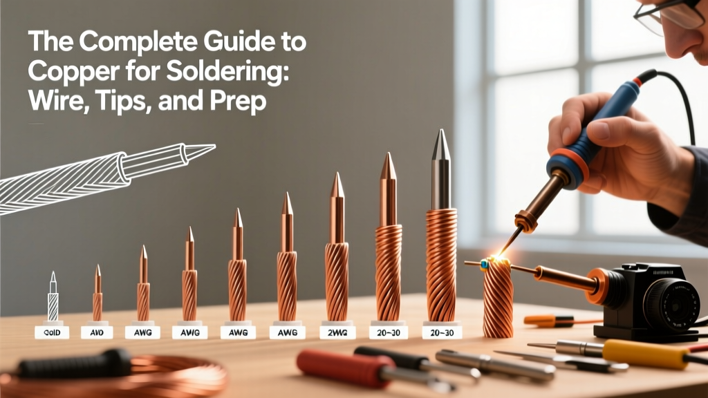
- Chisel Tips (e.g., Hakko T18-D24 or Weller ETA): The flat surface maximizes contact area with the component lead and the PCB pad simultaneously. Ideal for 0603 to 0805 SMT components and standard through-hole leads.
- Bevel / Hoof Tips (e.g., Hakko T18-C4): Features a concave cutout that holds a small reservoir of molten solder. Essential for drag-soldering fine-pitch (0.5mm) IC pins or soldering heavy ground planes that act as massive heat sinks.
- Knife Tips (e.g., Weller RTMS): Excellent for cleaning up solder bridges on QFN pads or reaching into tight mechanical clearances where a chisel tip would short adjacent vias.
As of 2026, active-tip stations like the Hakko FX-951 (approx. $245) or the Weller WX1021 (approx. $410) utilize embedded thermocouples within the tip itself, providing near-instantaneous thermal recovery. For heavy ground-plane joints, set the station to 350°C (662°F) with a massive bevel tip, rather than using a 400°C (752°F) needle tip which will instantly burn out and fail to transfer adequate joules to the copper.
The 4 Most Common Soldered Joint Defects
1. The Cold Joint
Visual Signature: Dull, grainy, grayish appearance with a convex, lumpy meniscus.
Root Cause: Insufficient heat transfer to the pad and lead before the solder melted, or movement during the plastic (cooling) phase. The flux failed to activate, leaving oxides intact.
Correction: Apply fresh ROL0 flux. Reheat the joint simultaneously on the pad and lead until the solder flows liquid, then remove heat and hold perfectly still.
2. The Disturbed Joint
Visual Signature: Frosty, wrinkled surface with visible micro-fissures.
Root Cause: Mechanical vibration or movement of the component while the solder was transitioning from liquid to solid (the plastic state). This physically tears the forming crystalline lattice.
Correction: Secure the PCB in a heavy vise or use a helping-hands tool with weighted bases. Reflow with additional flux.
3. Solder Starvation
Visual Signature: Flat, concave fillet that barely covers the pad, exposing the copper outline or failing to climb the component lead.
Root Cause: Insufficient solder volume applied, often seen when rushing or using wire that is too thin (e.g., using 0.015" wire on a 14 AWG terminal).
Correction: Feed additional 0.031" (0.8mm) diameter solder wire directly into the trailing edge of the iron tip until the fillet forms a smooth, concave curve up the lead.
4. Flux Inclusions & Outgassing Voids
Visual Signature: Small, dark pinholes or trapped bubbles visible within the solidified fillet or at the solder-mask boundary.
Root Cause: Rapid heating of high-solids flux, causing volatile solvents to boil and become trapped as the solder freezes around them.
Correction: Use a lower-activity, low-solids flux (e.g., Kester 186 RMA) and allow the iron to pre-heat the joint for 0.5 seconds before introducing the solder wire.
Flux Chemistry: The Unsung Hero of Wetting
You cannot achieve a reliable soldered joint without understanding flux. Flux chemically reduces metal oxides, allowing the molten solder to wet the copper. The IPC J-STD-004 standard classifies flux by composition and activity level.
- RO (Rosin): Derived from pine sap. RO L0 (Low activity, zero halides) is the standard for consumer and industrial electronics. Requires no-clean or mild solvent cleaning.
- OR (Organic): Water-soluble organic acids (OAs). Highly active, excellent for heavily oxidized vintage boards or thick mechanical lugs. Must be washed with deionized water post-soldering to prevent dendritic growth and electrochemical migration.
- IN (Inorganic): Contains strong acids (hydrochloric/zinc chloride). Used strictly for plumbing and heavy sheet metal. Never use on PCBs; it will rapidly corrode copper traces.
Expert Insight: When reworking a 5-year-old oxidized board, do not rely on the flux core inside your solder wire. It has likely degraded. Apply a generous amount of external liquid or tacky gel flux (like Amtech NC-559-V2-TF) directly to the joint before applying the iron.
Step-by-Step: Executing a Class 3 Through-Hole Joint
To achieve aerospace-grade reliability on a standard 0.062" FR4 board using SAC305 lead-free alloy, follow this exact thermal sequence:
- Preparation (0:00): Ensure the component lead is seated flush against the pad. Apply a small dab of ROL0 tack flux to the pad-lead intersection.
- Tip Placement (0:00 - 0:01): Place a clean, tinned 2.4mm chisel tip (set to 340°C) so it simultaneously touches the copper pad and the component lead. Hold for 1.0 second to establish thermal equilibrium.
- Feed Solder (0:01 - 0:02): Introduce 0.031" SAC305 solder wire to the opposite side of the joint (not directly onto the iron tip). The solder should melt instantly upon contacting the heated pad and wick up the lead via capillary action.
- Form the Fillet (0:02 - 0:03): Feed exactly enough solder to form a smooth, concave meniscus that climbs 75% up the lead. Total dwell time must not exceed 3.0 seconds to prevent pad delamination.
- Withdrawal (0:03 - 0:04): Remove the solder wire first, then pull the iron away at a 45-degree angle. This draws excess solder onto the tip and leaves a sharp, clean fillet peak.
- Inspection (Post-Cool): Verify the joint is shiny (or uniformly matte for lead-free), fully wetted, and free of micro-cracks under a 10x loupe.
Mastering the soldered joint requires shifting your mindset from "melting metal" to "managing thermal mass and metallurgical reactions." By adhering to strict IPC visual standards, selecting the correct tip geometry, and respecting flux chemistry, you will consistently produce joints that survive the harshest electrical and mechanical environments.