
The 2026 EMS Landscape: Miniaturization and High-Reliability
As we navigate 2026, the Electronics Manufacturing Services (EMS) sector is aggressively transitioning toward ultra-fine-pitch components. The proliferation of 01005 (0.4mm x 0.2mm) and the emerging 008004 (0.25mm x 0.125mm) metric passive components in aerospace, medical, and automotive ADAS (Advanced Driver Assistance Systems) modules demands unprecedented precision in industrial SMD soldering. For plant managers and process engineers, upgrading a surface mount technology (SMT) line is no longer just about throughput; it is about achieving zero-defect manufacturing under strict IPC-A-610 Class 3 compliance.
This comprehensive buyer's guide dissects the critical capital equipment, metallurgical considerations, and thermal profiling strategies required to build a high-yield SMD soldering line in 2026. Whether you are scaling an existing facility or greenfielding a new high-reliability production floor, the decisions made regarding your reflow, inspection, and material handling ecosystems will dictate your first-pass yield (FPY) for the next decade.
Core Industrial SMD Soldering Equipment Matrix
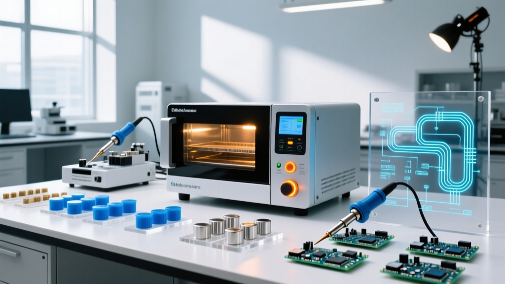
Selecting the right machinery requires balancing capital expenditure (CapEx) against the specific component density of your product mix. Below is a comparative matrix of top-tier industrial equipment dominating the 2026 EMS market.
| Equipment Category | 2026 Industry Standard Model | Estimated CapEx Range | Primary Application & ROI Driver |
|---|---|---|---|
| Reflow Oven | Heller 1809EXL (9-Zone) | $85,000 - $115,000 | Nitrogen-inerted reflow for SAC305 and low-temp alloys; reduces oxidation and voiding. |
| Pick and Place | Yamaha YRM20 | $160,000 - $210,000 | High-speed, high-mix placement (46,000 CPH); essential for 01005 and micro-BGA accuracy. |
| SPI (Solder Paste Inspection) | Koh Young Zenith | $95,000 - $130,000 | 3D profilometry to detect paste volume and bridging defects pre-reflow; critical for FPY. |
| Selective Soldering | EBSO SPA 450 | $120,000 - $155,000 | Automated through-hole soldering on mixed-tech boards without the thermal shock of wave soldering. |
Deep Dive: The Necessity of 3D SPI in Modern SMD Lines
In 2026, relying solely on post-reflow Automated Optical Inspection (AOI) is a financial liability. Industry data from the Surface Mount Technology Association (SMTA) consistently shows that up to 70% of all SMD soldering defects originate in the stencil printing phase. A high-end 3D SPI system like the Koh Young Zenith utilizes digital fringe projection to measure solder paste volume, area, height, and offset with sub-micron accuracy. For 01005 components, where the required paste volume is measured in nanoliters, detecting a 15% volume deficit before the component is ever placed saves massive rework costs and prevents latent field failures.
Solder Paste Metallurgy and Stencil Engineering
The physical hardware of your SMT line is only as effective as the consumables running through it. Industrial SMD soldering requires a meticulous alignment of solder paste particle size, flux chemistry, and stencil aperture design.
Paste Typing: Matching Particle Size to Component Pitch
As component footprints shrink, the spherical metal powder in the solder paste must scale accordingly to prevent solder balling and bridging. The IPC J-STD-005 standard defines these classifications:
- Type 3 (25-45 µm): Legacy applications, standard 0805 and 1206 passives, and coarse-pitch QFPs.
- Type 4 (20-38 µm): The current baseline for 0402 components and standard BGAs with 0.5mm pitch.
- Type 5 (15-25 µm): Mandatory for 0201 components, 0.4mm pitch micro-BGAs, and fine-pitch QFNs.
- Type 6 (5-15 µm): Reserved for ultra-fine 01005 and 008004 passives, and 0.3mm pitch CSPs (Chip Scale Packages).
Expert Note: Upgrading from Type 4 to Type 5 paste increases the surface area of the solder powder, which inherently accelerates oxidation. If you run Type 5 or Type 6 pastes, a nitrogen-inerted reflow oven (maintaining <50 ppm O2) is not optional; it is a strict requirement to prevent gross solder balling and non-wetting.
Stencil Thickness and Nano-Coatings
For high-reliability mixed-technology boards, a stepped stencil is often required. A standard 4-mil (100 µm) thickness works for larger ICs, but applying 01005 passives requires a 3-mil (75 µm) or even 2-mil (50 µm) stepped-down pocket to prevent paste volume overage. Furthermore, in 2026, applying a nano-coating (such as NanoSlic or G Nano) to the stencil's squeegee side and aperture walls is standard practice for Class 3 medical and automotive builds. These hydrophobic coatings improve paste transfer efficiency (TE) from an average of 75% to over 92%, drastically reducing the need for manual stencil wiping and minimizing micro-bridging.
Thermal Profiling for High-Reliability (Class 3) Compliance
Achieving compliance with IPC J-STD-001 requires a thermal profile that ensures complete intermetallic compound (IMC) formation without exceeding the thermal degradation limits of sensitive components or the PCB's Tg (glass transition temperature). For standard SAC305 (Sn96.5/Ag3.0/Cu0.5) lead-free alloy, the liquidus temperature is 217°C.
'The most common failure mode in modern high-density SMD soldering is not cold solder joints, but thermal damage to the PCB laminate and component delamination caused by aggressive ramp rates. A controlled soak is non-negotiable for Class 3 assemblies.' — Senior Process Engineer, Tier 1 Automotive EMS.
The Optimal Ramp-Soak-Spike (RSS) Profile
- Preheat / Ramp (Room Temp to 150°C): Maintain a ramp rate of 1.5°C to 2.5°C per second. Exceeding 3°C/sec risks fracturing ceramic capacitors (MLCCs) due to thermal shock and can cause solder paste spattering.
- Soak Zone (150°C to 200°C): Hold for 60 to 90 seconds. This allows the flux activators (typically ROL0 or ROL1 chemistries) to volatilize and clean the oxidation from the component terminations and PCB pads. It also equalizes the temperature across the board, preventing shadowing effects near large thermal mass components like power inductors.
- Reflow / Spike (Above 217°C): Time above liquidus (TAL) should be strictly controlled between 45 and 75 seconds. Peak temperature should hit 235°C to 245°C. This ensures a robust Cu6Sn5 and Ni3Sn4 intermetallic layer forms at the joint interface.
- Cooling Zone: A rapid but controlled cooling rate of 3°C to 5°C per second promotes a fine-grain microstructure in the solder joint, which increases mechanical fatigue resistance and drop-shock survivability.
Critical Defect Mitigation Strategies
Even with top-tier 2026 equipment, specific failure modes plague high-density SMD soldering. Understanding the root cause of these defects is vital for process optimization.
Head-in-Pillow (HiP) Defects
Head-in-Pillow occurs when the solder paste on the PCB pad and the solder sphere on the BGA component melt, but fail to coalesce into a single homogeneous joint. Visually, it looks like a head resting on a pillow. This is predominantly caused by BGA warpage during the reflow process or severe oxidation on the BGA spheres. Solution: Utilize a Type 5 solder paste with a highly active flux chemistry (ROL1) and implement a pre-tacking process using a dip-flux station before BGA placement to guarantee oxide removal.
Tombstoning on 0201 and 01005 Passives
Tombstoning happens when one side of a passive component wets before the other, and the surface tension of the molten solder pulls the component upright. Solution: This is almost always a thermal imbalance issue. Ensure the PCB pad design is perfectly symmetrical. If one pad connects to a massive ground plane and the other to a thin trace, the ground plane will act as a heatsink, delaying reflow on that side. Use thermal relief spokes on ground plane connections and verify your reflow oven's cross-conveyor temperature uniformity is within ±2°C.
CapEx Planning and Line Integration
Outfitting a complete, state-of-the-art SMD soldering line in 2026 requires a CapEx investment ranging from $800,000 for a standard mid-volume line to over $2.5 million for a fully automated, lights-out high-reliability cell. When calculating ROI, factor in the hidden costs of nitrogen generation (if not supplied via bulk liquid tanks), compressed air drying systems, and the ongoing licensing for SPC (Statistical Process Control) software that bridges your SPI, Pick-and-Place, and AOI machines into a unified closed-loop manufacturing execution system (MES).
Ultimately, success in industrial SMD soldering hinges on the synergy between precision machinery, rigorous metallurgical science, and uncompromising adherence to IPC standards. By investing in 3D inspection, nitrogen-inerted reflow, and advanced stencil engineering, EMS providers can secure the high-yield, zero-defect production required by today's most demanding technology sectors.