
The Standard for High-Reliability Manufacturing
In the realm of industrial electronics and aerospace manufacturing, soldering is not merely a mechanical connection; it is a precise metallurgical bond. Unlike hobbyist projects where a functional joint is sufficient, industrial applications demand strict adherence to the latest IPC-A-610 and IPC-J-STD-001 Class 3 (High-Reliability) standards. A failure in a medical device, automotive control unit, or satellite telemetry board is unacceptable. This guide details the exact step by step soldering process required to achieve zero-defect assemblies in high-stakes manufacturing environments, utilizing modern thermal management techniques and advanced metallurgical principles.
Industrial Soldering Equipment: Beyond the Hobbyist Bench
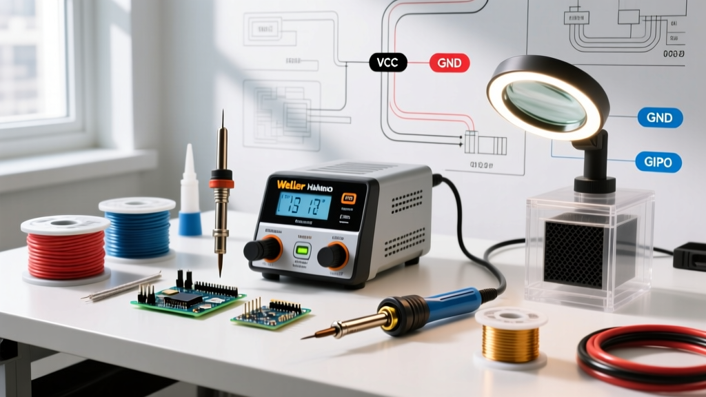
Before initiating the step by step soldering process, operators must utilize equipment capable of rapid thermal recovery and precise profiling. Standard ceramic-heater irons suffer from thermal lag, leading to cold joints on multi-layer boards with heavy ground planes.
- RF SmartHeat Stations: Systems like the Metcal MX-5200 (priced around $950-$1,100) use high-frequency electromagnetic fields to heat the tip directly via the skin effect. This provides instantaneous thermal recovery without the need for manual temperature calibration.
- Cartridge-Based Systems: The JBC CD-2BQF (approximately $800-$900) features an integrated heater in the tip cartridge, reducing the thermal distance between the heating element and the solder joint to near zero. This allows for lower idle temperatures (e.g., 350°C instead of 400°C), drastically extending tip life and reducing thermal shock to sensitive SMD components.
- Flux and Solder Alloys: Industrial environments heavily favor SAC305 (Sn96.5Ag3.0Cu0.5) for lead-free compliance, or Sn63Pb37 for exempted high-reliability aerospace applications. Flux selection typically involves low-solids, no-clean formulations (like Kester 275) or water-soluble organic acid (OA) fluxes for high-activity cleaning post-soldering.
The Step by Step Soldering Process for Class 3 Assemblies
Executing a flawless through-hole or surface mount rework joint requires a disciplined, sequential approach. Below is the definitive industrial workflow.
Step 1: Substrate Preparation and Moisture Management
Before any heat is applied, verify the Moisture Sensitivity Level (MSL) of the components. If components have exceeded their floor life, they must be baked at 125°C for 4 to 24 hours to prevent the 'popcorn effect' (internal delamination and cracking) during soldering. Clean the PCB pads using a lint-free wipe and high-purity Isopropyl Alcohol (IPA) or a specialized saponifier to remove oxidation and handling oils.
Step 2: Tip Selection and Pre-Tinning
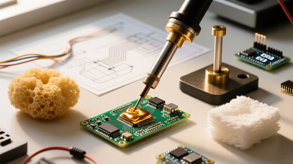
Select a tip geometry that maximizes contact area without bridging adjacent pads. For a standard 0805 SMD component, a chisel tip (e.g., JBC C245-945) is ideal. Apply a small amount of fresh, flux-cored solder to the tip immediately upon heating. This 'pre-tinning' creates a liquid thermal bridge, increasing heat transfer efficiency by up to 40% compared to a dry, oxidized tip.
Step 3: Thermal Transfer and Flux Activation
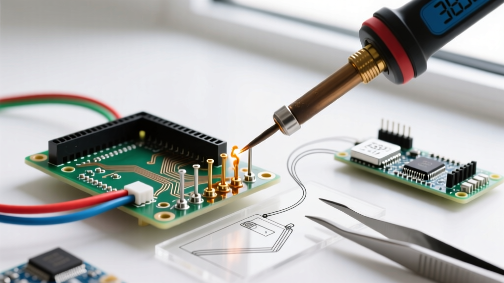
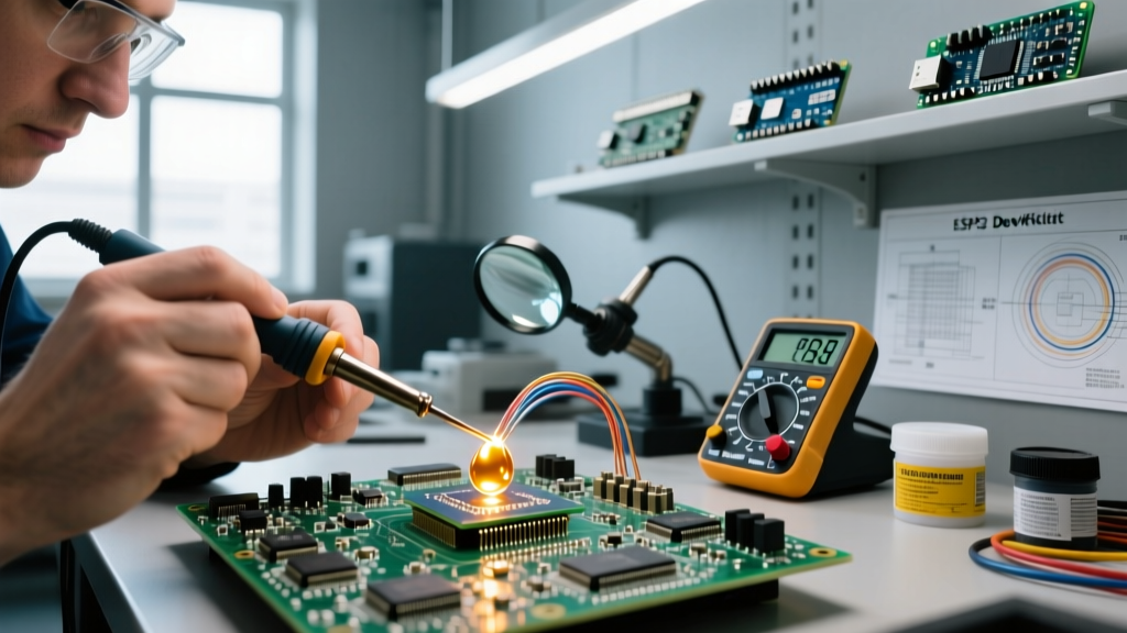
Place the tinned tip simultaneously on the PCB pad and the component lead. Hold for 1 to 1.5 seconds. This critical dwell time allows the flux core to melt, flow, and activate. The flux must reach its activation temperature (typically 150°C–180°C for no-clean rosin-based fluxes) to chemically reduce metal oxides before the bulk solder melts.
Step 4: Solder Delivery and Wetting
Feed the solder wire directly into the joint interface—never melt the solder on the iron tip and carry it to the joint. Carrying molten solder depletes the flux through premature volatilization, leading to poor wetting and graping. Deliver the precise volume required to form a concave fillet with a wetting angle of less than 90 degrees, as mandated by IPC-A-610.
Step 5: Controlled Solidification
Remove the solder wire first, then the iron tip. Allow the joint to cool naturally. In industrial settings, operators must never blow on the joint or use forced air cooling, as this induces micro-cracking in the intermetallic compound (IMC) layer and creates a disturbed joint, which is an automatic Class 3 defect.
Thermal Profiling and Alloy Selection Matrix
Understanding the thermal boundaries of your specific alloy is critical to preventing pad delamination and component damage. The following matrix outlines standard operating parameters for industrial hand-soldering.
| Alloy Composition | Melting Point | Optimal Iron Temp | Max Dwell Time | Primary Application |
|---|---|---|---|---|
| SAC305 (Lead-Free) | 217°C - 220°C | 350°C - 380°C | 3.0 Seconds | Commercial / Industrial (RoHS) |
| Sn63Pb37 (Eutectic) | 183°C | 315°C - 330°C | 4.0 Seconds | Aerospace / Medical (Exempt) |
| Sn96.3Ag3.0Cu0.7 | 217°C | 360°C - 390°C | 2.5 Seconds | High-Vibration Automotive |
| Sn42Bi57.6Ag0.4 | 138°C - 139°C | 240°C - 260°C | 4.0 Seconds | Low-Temp / Heat-Sensitive |
Expert Insight: When transitioning from leaded to lead-free SAC alloys, operators often mistakenly increase their iron temperature to 420°C+ to compensate for the higher melting point. This is a critical error. Excessive tip temperatures rapidly degrade the iron plating and scorch the flux, resulting in severe voiding. Instead, rely on the rapid thermal recovery of modern RF stations and increase the tip size, not the temperature.
Edge Cases and Advanced Failure Mode Troubleshooting
Even with a flawless step by step soldering process, complex multi-layer PCBs introduce thermal mass disparities that can cause specific failure modes. Recognizing and mitigating these edge cases separates novice technicians from certified IPC specialists.
Tombstoning in SMD Passives
Tombstoning occurs when a small surface-mount component (like a 0402 capacitor) stands on one end during reflow or hand-tack soldering. This is caused by unequal wetting forces. If one pad is connected to a heavy internal ground plane, it acts as a heat sink, delaying the melting of the solder paste or wire on that side. Correction: Pre-heat the larger thermal mass pad with the iron for 0.5 seconds before applying solder, or use a localized pre-heater (like a PACE PH-100) set to 100°C to elevate the entire board's baseline temperature.
Intermetallic Compound (IMC) Overgrowth
A solder joint's mechanical strength relies on a thin, continuous IMC layer (typically Cu6Sn5) between the copper pad and the bulk solder. If the dwell time exceeds 4-5 seconds, or if the joint is repeatedly reworked, the IMC layer grows excessively thick and becomes brittle, leading to catastrophic fracture under thermal cycling or mechanical shock. According to research published by NASA's Electronic Parts and Packaging (NEPP) Program, controlling thermal exposure is the single most critical factor in ensuring long-term solder joint reliability in spaceflight hardware.
Pad Lift and Laminate Degradation
FR-4 laminates have a Glass Transition Temperature (Tg). Standard FR-4 has a Tg of ~135°C, while high-Tg materials (like Isola 370HR) operate at 170°C+. Prolonged exposure to 380°C soldering irons can cause the Z-axis expansion of the PCB to exceed the tensile strength of the copper-to-resin bond, resulting in pad lift. Always utilize thermal profiling data provided by organizations like SMT007 to ensure your hand-soldering parameters do not compromise the structural integrity of high-density interconnect (HDI) boards.
Verification and Final Inspection
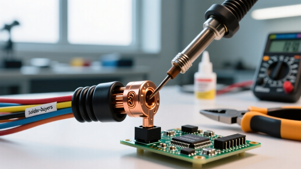
The final phase of the industrial soldering workflow is rigorous inspection. Utilizing a stereo zoom microscope (such as the AmScope SM-4TP) at 10x to 30x magnification, verify the following IPC-A-610 Class 3 criteria:
- Fillet Shape: Must be concave with a smooth, continuous transition from the pad to the component lead.
- Wetting Angle: Must be less than 90 degrees, indicating proper flux activation and oxide removal.
- Solder Volume: The lead outline must be discernible through the solder fillet; excessive solder obscuring the lead is classified as a defect.
- Cleanliness: If using no-clean flux, residue must not be excessive or corrosive. If using water-soluble flux, the board must undergo an ultrasonic or saponifier wash within 2 hours to prevent dendritic growth and electrochemical migration (ECM).
By strictly adhering to this step by step soldering process, manufacturers ensure that every joint meets the rigorous demands of modern industrial electronics. For comprehensive guidelines on acceptability criteria, technicians should continually reference the official documentation provided by IPC (Association Connecting Electronics Industries), which remains the global benchmark for electronic assembly quality.