
The Anatomy of a Good Soldering Joint: An Expert Roundup
Ask a novice what makes a good soldering joint, and they will likely tell you it needs to be "shiny and smooth." Ask an IPC-certified master trainer or an aerospace soldering engineer, and you will get a vastly different answer involving intermetallic compounds, wetting angles, and thermal profiling. In modern electronics manufacturing and high-reliability DIY repair, visual appeal is merely a byproduct of correct metallurgical bonding.
To separate myth from metallurgical fact, we have synthesized insights from three distinct domains of soldering expertise: Aerospace Workmanship (NASA standards), Commercial Electronics Assembly (IPC guidelines), and Thermal Dynamics Engineering (tooling manufacturers). Whether you are hand-soldering a 0402 SMD capacitor or reworking a heavy through-hole power connector, understanding the exact criteria of a good soldering joint is critical for long-term reliability.
The Aerospace Perspective: NASA-STD-8739.3 Strictness
In aerospace and mission-critical applications, a solder joint must survive extreme thermal cycling, vibration, and vacuum conditions. According to experts who train to the NASA Workmanship Standards, a good soldering joint is defined by absolute predictability.
Expert Insight: "In Class 3 and aerospace applications, we do not accept 'hidden' connections. A good through-hole joint must exhibit a 360-degree wetted barrel with a visible, concave meniscus on both the top and bottom of the PCB. The solder must feather out to a zero-degree edge, proving that the copper pad was properly heated and the flux fully activated."
For aerospace engineers, the absence of voids and the presence of a smooth, continuous fillet are non-negotiable. Any sign of graininess indicates the joint was disturbed during the critical phase-change window between the liquidus and solidus temperatures, creating a micro-fracture network that will fail under vibration.
The Commercial Baseline: IPC-A-610 Rev H Criteria
For commercial and industrial electronics, the IPC-A-610 Acceptability of Electronic Assemblies standard is the undisputed global benchmark. IPC Master Trainers evaluate a good soldering joint based on three tiers: Target (ideal), Acceptable (reliable), and Defect (unreliable).
Key Wetting Angle Requirements
Wetting is the ability of molten solder to flow and adhere to the base metal. Experts emphasize that the contact angle (where the solder meets the pad) is the ultimate truth-teller.
- Target Condition: A wetting angle of less than 45 degrees, indicating excellent capillary action and robust Intermetallic Compound (IMC) formation.
- Acceptable (Class 2): A wetting angle up to 90 degrees is permitted, provided there is clear evidence of wetting and no non-wetting or dewetting areas.
- Defect: An angle greater than 90 degrees, or a "balling" effect where the solder pulls away from the pad edges (dewetting), signaling oxidation or inadequate thermal transfer.
Comparative Matrix: Inspecting the Good Soldering Joint
The definition of "good" shifts depending on the component topology and the reliability class of the end product. Below is an expert-compiled inspection matrix for the most common joint types.
| Joint Type | IPC Class 2 (Standard) | IPC Class 3 (High-Rel) | Common Failure Mode |
|---|---|---|---|
| Through-Hole (Leaded) | 75% barrel fill; wetting on solder side | 100% barrel fill; 360° wetting both sides | Cold barrel; flux entrapment |
| SMD Gullwing (SOIC/QFP) | Toe fillet visible; side fillet > 1x lead width | Toe, heel, and side fillets fully formed | Heel fillet starvation; tombstoning |
| SMD Chip (0402/0603) | Fillet visible on one end; wetted to terminal | Fillets on both ends; concave profile | Tombstoning; solder bridging |
| BGA (Ball Grid Array) | X-ray: uniform sphere, no bridging | X-ray: uniform sphere, <25% voiding | Head-in-Pillow (HiP); micro-voiding |
The Metallurgy of a Good Soldering Joint: IMC Formation
You cannot see the most important part of a good soldering joint with the naked eye. According to metallurgical experts, the true strength of a solder connection lies in the Intermetallic Compound (IMC) layer. When molten SAC305 (Sn96.5/Ag3.0/Cu0.5) or Sn63Pb37 (Eutectic) solder contacts a copper pad, a chemical reaction occurs, forming Cu6Sn5 and eventually Cu3Sn.
The Goldilocks Zone of IMC Thickness
- Too Thin (< 0.5 µm): Indicates insufficient heat or time. The joint lacks mechanical strength and is prone to shear failure.
- Ideal (1.0 µm - 3.0 µm): Achieved with proper thermal profiling (typically 1.5 to 3.0 seconds of dwell time at the pad). Provides optimal tensile and shear strength.
- Too Thick (> 5.0 µm): Caused by excessive heat or prolonged rework. The IMC layer becomes brittle and glass-like, leading to catastrophic cracking under thermal or mechanical shock.
This is why experts vehemently advise against "cooking" a joint. Keeping a 400°C iron on a pad for 10 seconds will yield a thick, brittle IMC layer, even if the joint looks perfectly shiny on the outside.
Thermal Profiling: Avoiding the "Shiny but Brittle" Trap
Tooling engineers from companies like Hakko and Weller emphasize that a good soldering joint is impossible without proper thermal management. As detailed in Hakko's technical guides on thermal recovery, the iron tip must transfer heat to both the pad and the lead simultaneously to activate the flux before the solder flows.
Expert Tooling Recommendations for 2026
- Ditch the Conical Tip: Conical (pointed) tips have terrible thermal mass transfer. Experts recommend chisel or bevel tips (e.g., Hakko T18-D24 or Weller RT4) to maximize surface area contact.
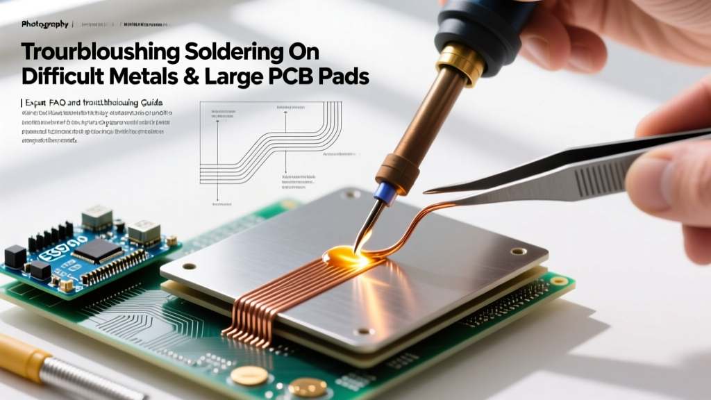
- Match the Thermal Mass: Soldering a 14-pin SOIC requires a different tip than a 10AWG XT60 connector. Using a micro-tip on a ground plane will result in a cold joint because the PCB acts as a massive heatsink, pulling heat away faster than the iron can replenish it.
- Use the Right Flux Chemistry: For hand soldering, ROL0 (Rosin, Low Activity, 0% Halides) or ROL1 no-clean fluxes are preferred. They activate around 150°C–180°C, cleaning oxides just before the solder reaches its liquidus point.
Troubleshooting Edge Cases: When "Good" Fails
Even experienced technicians encounter edge cases where a joint appears acceptable but harbors latent defects. Here is how experts diagnose the most deceptive failure modes.
1. The Disturbed Joint (Grainy/Frosted Appearance)
The Cause: The component or PCB was moved while the solder was cooling through the plastic (semi-solid) phase between liquidus and solidus temperatures.
The Fix: Do not simply add more solder. Apply fresh flux, reflow the joint completely to allow the crystalline structure to reset, and hold the component perfectly still for 2-3 seconds until the solder fully solidifies.
2. Dewetting (Solder Pulls Back from Pad Edges)
The Cause: The pad was initially wetted, but the solder subsequently retreated, leaving a thick blob surrounded by a thin, oxidized film. This is often caused by severe pad contamination (silicone, oils) or excessive iron temperature burning the flux before it could clean the metal.
The Fix: Clean the pad with isopropyl alcohol (IPA) and a lint-free swab. Apply a generous amount of high-activity water-soluble or RA (Rosin Activated) flux, lower the iron temperature by 20°C, and reflow using a wider chisel tip.
3. Pad Lift and Delamination
The Cause: Exceeding the glass transition temperature (Tg) of the FR-4 substrate for too long. Standard FR-4 has a Tg of 130°C–140°C, and pad peel strength drops exponentially above 260°C.
The Fix: If a pad lifts, stop immediately. A lifted pad cannot be pushed back down reliably. The expert repair method involves scraping the solder mask off the connected trace, tinning the exposed copper, and using a 30AWG bare copper wire to stitch the component lead directly to the trace, securing it with UV-curable solder mask resin.
Final Verdict: The Hallmarks of Mastery
Ultimately, a good soldering joint is a testament to controlled chemistry and precise thermodynamics. It features a concave fillet, a wetting angle well under 90 degrees, complete barrel fill (for through-hole), and an IMC layer strictly between 1 and 3 microns thick. By shifting your focus from "making it look shiny" to "managing heat transfer and flux activation," you align your workbench practices with the rigorous standards demanded by aerospace and commercial IPC inspectors.