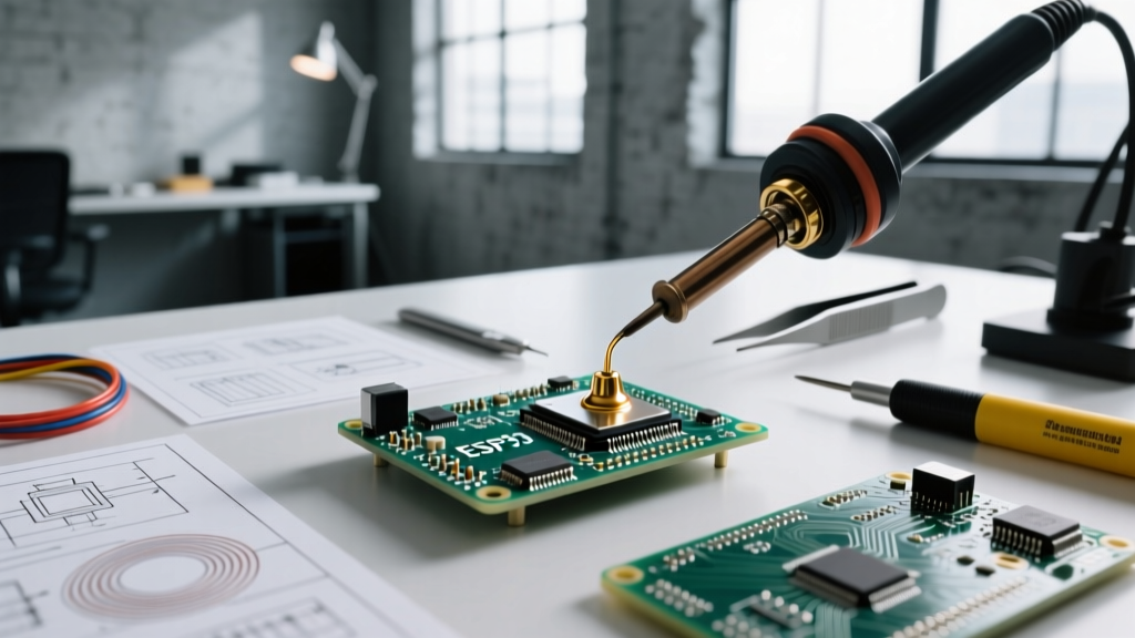

The Myth of the Universal Soldering Temperature
If you ask a dozen hobbyists what their default soldering temp for electronics is, you will likely hear "350 degrees" repeated like a mantra. While 350°C is a safe middle ground for general-purpose lead-free soldering, treating it as a universal constant is a fundamental misunderstanding of thermal dynamics. In professional PCB assembly and advanced DIY prototyping, the correct temperature is never a static number; it is a dynamic variable dictated by alloy composition, thermal mass, and component sensitivity.
As of 2026, with the widespread adoption of complex multi-layer boards and temperature-sensitive SMD components like MLCCs (Multi-Layer Ceramic Capacitors), applying excessive heat is just as destructive as applying too little. This decision framework will help you systematically determine the exact soldering temp for electronics based on your specific project parameters, ensuring strong intermetallic bonds without causing thermal damage to the PCB substrate or silicon dies.
The Physics of the Solder Joint: Melting Point vs. Tip Temperature
Before setting your station dial, you must differentiate between the melting point of the solder alloy and the tip temperature required to create a reliable joint. The goal of soldering is not merely to melt the wire; it is to heat the pad and the component lead to a temperature that allows the flux to clean the oxidation and the molten solder to wet the surfaces, forming an Intermetallic Compound (IMC) layer.
Expert Insight: The ideal IMC layer thickness for a reliable joint is between 1 and 3 microns. Prolonged exposure to excessive heat causes the IMC layer to overgrow, making the joint brittle and prone to mechanical failure under vibration or thermal cycling.
To achieve proper wetting within the recommended 2 to 4 seconds per joint (as outlined by IPC standards), your iron tip must be significantly hotter than the alloy's liquidus temperature to compensate for the instantaneous heat sink effect of the copper pad and component lead.
Baseline Matrix: Soldering Temp by Alloy Composition
Your primary variable is the solder alloy. The table below provides the baseline starting temperatures for the most common electronics solders used today.
| Solder Alloy | Composition | Melting Point (Liquidus) | Baseline Tip Temp | Primary Use Case |
|---|---|---|---|---|
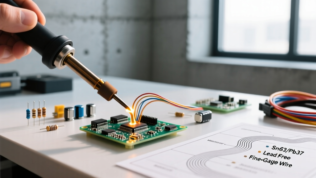
| Sn63/Pb37 | 63% Tin / 37% Lead | 183°C (361°F) | 300°C - 320°C | Prototyping, vintage repair, aerospace |
| SAC305 | 96.5% Sn / 3% Ag / 0.5% Cu | 217°C (423°F) | 340°C - 360°C | Standard commercial lead-free SMD/TH |
| Sn42/Bi57 | 42% Tin / 58% Bismuth | 138°C (280°F) | 220°C - 250°C | Low-temp repairs, heat-sensitive flex PCBs |
| Sn96.5/Ag3.5 | 96.5% Tin / 3.5% Silver | 221°C (430°F) | 350°C - 370°C | High-reliability, high-vibration joints |
Note: Always consult the specific datasheet for your solder wire. Flux core formulations vary, and some activate at lower temperatures than others. Refer to manufacturer guidelines like those found in the Hakko Technical Tips library for alloy-specific flux activation windows.
The 4-Step Decision Framework
Use this sequential framework to dial in your station (such as a Pace ADS200, JBC CD-2BE, or Weller WE1010) for any given board.
Step 1: Establish the Alloy Baseline
Identify your solder wire. If you are using Sn63/Pb37, set your station to 310°C. If using SAC305, set it to 350°C. This is your starting point, not your final destination.
Step 2: Assess the Thermal Mass of the Joint
Thermal mass is the enemy of temperature. A 0402 resistor on a 2-layer board has very low thermal mass; the baseline temperature will work perfectly. However, a TO-220 voltage regulator tab connected to an internal ground plane on a 4-layer board acts as a massive heat sink.
- Low Thermal Mass (0402 to 0805 SMDs, small signal TH): Keep baseline temp. Do not exceed 3 seconds of contact.
- Medium Thermal Mass (1206 SMDs, standard DIP ICs, 0.1" headers): Baseline temp is usually sufficient, provided you are using a correctly sized chisel or bevel tip.
- High Thermal Mass (Large ground vias, RF shields, power connectors): Do not simply increase the temperature to 400°C to compensate. This will burn the flux and delaminate the FR-4 substrate. Instead, increase the tip size (use a heavy bevel or wide chisel) to maximize surface area contact, or use a PCB pre-heater to bring the ambient board temperature up to 100°C before applying the iron.
Step 3: Evaluate Component Sensitivity
Certain components are highly susceptible to thermal shock or absolute temperature limits.
- MLCCs (Multi-Layer Ceramic Capacitors): Prone to micro-cracking if subjected to rapid localized heating. Use a slightly lower temperature (e.g., 300°C for leaded) and a wide bevel tip to heat the pad and component terminations simultaneously and evenly.
- Plastic Connectors (JST, Molex, FPC/FFC): The housing melts easily. Use a lower temperature (280°C - 300°C) and a fine conical or micro-chisel tip to apply heat strictly to the metal pin, avoiding the plastic shroud.
- RF Modules and Shielded Cans: The solder used to attach the shield often requires high heat. Use a dedicated heavy-duty tip at 380°C to melt the shield ground tabs quickly without transferring prolonged heat to the sensitive RF ICs inside.
Step 4: Select the Correct Tip Geometry
Temperature is useless without thermal transfer. A 400°C micro-conical tip (often mistakenly called a "precision" tip) will transfer less actual heat energy to a joint than a 320°C wide chisel tip. The conical tip touches the pad with a microscopic point, creating a massive thermal bottleneck. Always use the largest tip geometry that fits the pad. Chisel and bevel (hoof) tips provide superior thermal coupling due to increased surface area contact.
Edge Cases and Failure Modes
When the soldering temp for electronics is miscalibrated, the physical evidence left on the PCB tells a clear story. Recognizing these failure modes allows you to adjust your framework in real-time.
1. Flux Burn-Off and Charred Residues
Symptom: The flux spatters violently, turns black, and leaves a hard, crusty residue that is difficult to clean with isopropyl alcohol.
Cause: Tip temperature is too high (typically above 380°C for standard rosin-based fluxes), or the iron was left on the joint for too long.
Correction: Drop the temperature by 20°C and verify your tip is properly tinned. A dry tip acts as an insulator, forcing the user to hold the iron longer, which eventually burns the flux.
2. The Classic Cold Joint
Symptom: The solder forms a dull, gray, grainy ball that does not wet the pad or lead (often resembling a raspberry).
Cause: Insufficient heat transfer. The solder melted from the iron tip, but the pad and component lead never reached the wetting temperature.
Correction: Check your tip geometry. If you are using a conical tip, switch to a chisel. Ensure you are heating the pad and the lead simultaneously for 1-2 seconds before introducing the solder wire.
3. Pad Lifting and Substrate Delamination
Symptom: The copper pad detaches from the fiberglass substrate, or the solder mask blisters and peels away from the via.
Cause: Excessive temperature combined with prolonged dwell time. Standard FR-4 has a Glass Transition Temperature (Tg) of around 130°C to 140°C. While it can withstand brief spikes to 260°C during reflow, holding a 380°C iron on a pad for 10 seconds will destroy the epoxy resin bond.
Correction: If a joint is not flowing within 4 seconds, remove the iron. Let the board cool, apply fresh flux, and try again with a larger tip or a pre-heater. Consult NASA Workmanship Standards for strict guidelines on maximum allowable rework thermal profiles.
Verification: Trust, But Calibrate
Modern digital soldering stations are highly accurate, but the temperature displayed on the LCD is the temperature of the heating element inside the handpiece, not the extreme tip of the copper barrel. Oxidation, loose tip sleeves, and degraded heating cores can cause a discrepancy of 20°C to 50°C between the display and the actual working surface.
For serious electronics work, invest in a tip thermometer (such as the Hakko FG-100B or Pace PTT-1). These devices use a specialized thermocouple sensor with a thermal pad to measure the exact surface temperature of your tip. Calibrating your station's offset based on a physical tip thermometer reading is the final, critical step in ensuring your decision framework yields consistent, professional-grade results.
Summary Checklist for the Workbench
- Identify Alloy: Set baseline temp (e.g., 310°C for Sn63/Pb37, 350°C for SAC305).
- Evaluate Mass: Use larger tips for ground planes; use pre-heaters instead of cranking the dial to 400°C.
- Protect Components: Lower temps and use wide bevel tips for MLCCs to prevent thermal shock.
- Ditch the Cone: Replace micro-conical tips with chisels or bevels for 90% of your SMD and through-hole work.
- Time Limit: Target 2 to 4 seconds of dwell time per joint. If it takes longer, change the tip, not the temperature.