
The Modern PCB Assembly Landscape
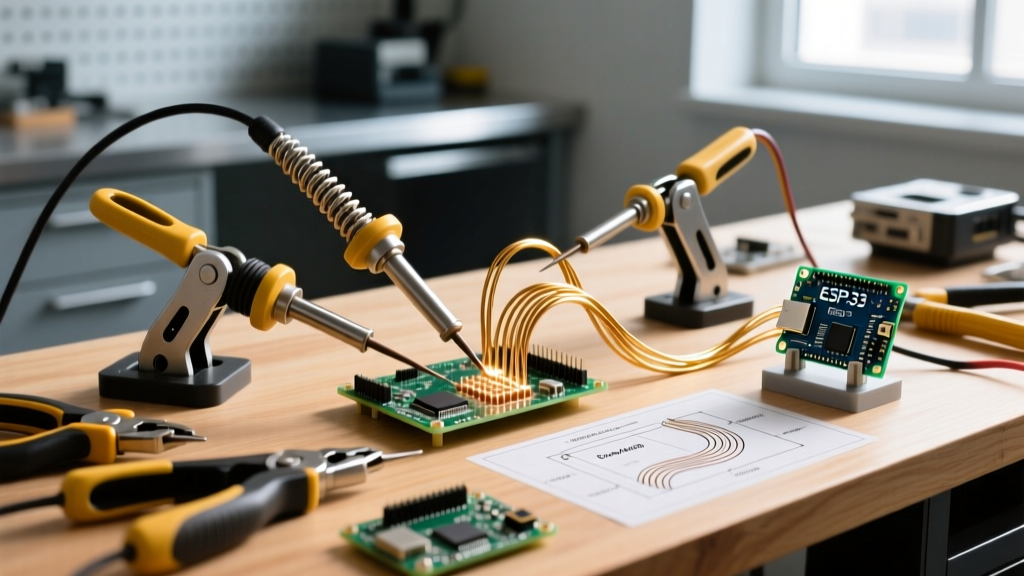
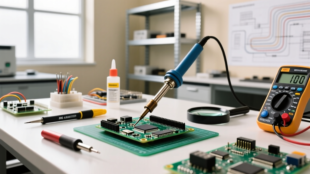
As we navigate the electronics landscape in 2026, the miniaturization of components and the rise of high-density interconnect (HDI) boards have made selecting the right soldering techniques more critical than ever. Whether you are a hobbyist prototyping an ESP32-based IoT sensor or a small-batch manufacturer producing 500 units of a mixed-signal RF board, applying the wrong thermal method can lead to catastrophic pad lift, tombstoning, or hidden micro-cracks.
This guide provides a comprehensive decision framework to help you evaluate and select the optimal soldering techniques based on component geometry, production volume, thermal mass, and budget constraints.
The Core Decision Matrix
Before picking up an iron or programming a reflow profile, map your project requirements against this foundational matrix. This table serves as your initial filter for choosing the appropriate methodology.
| Soldering Technique | Optimal Component Types | Estimated Setup Cost (2026) | Minimum Pitch Capability | Ideal Batch Size |
|---|---|---|---|---|
| Hand Soldering (THT) | Leaded resistors, capacitors, connectors | $100 - $150 | 2.54mm (Standard) | 1 - 50 units |
| Drag Soldering (SMD) | SOIC, TQFP, fine-pitch QFP | $120 - $200 | 0.5mm | 1 - 20 units |
| Hot Air Rework | QFN, DFN, large SMD passives, BGAs | $200 - $350 | 0.4mm (with stencil) | Prototyping / Repair |
| DIY Reflow (Hotplate/Oven) | Mixed SMD, dense 0402/0201 layouts | $150 - $300 | 0.3mm (BGA) | 10 - 200 units |
| Micro-Soldering | 01005 passives, BGA reballing | $800 - $1,500+ | 0.15mm | Specialized Repair |
Through-Hole Technology (THT): The Baseline
Despite the dominance of surface mount technology, through-hole components remain essential for high-current paths, mechanical stress points (like USB-C connectors), and high-voltage isolation. The primary technique here is manual hand soldering using a temperature-controlled station.
Tooling and Thermal Mass Management
For standard THT work, the IPC J-STD-001 standard dictates that the solder joint must reach the liquidus temperature of the alloy within 2 to 5 seconds. To achieve this without damaging the board, you need a station with high thermal recovery. The Weller WE1010NA (approx. $125) or the Hakko FX-888D (approx. $115) remain the gold standards for DIYers and light commercial use.
- For standard 1/4W resistors: Use a 2.4mm chisel tip (e.g., Hakko T18-D24) set to 320°C for lead-free SAC305 wire.
- For heavy ground planes: Do not simply turn up the temperature, which oxidizes the tip. Instead, switch to a high-capacity bevel tip (e.g., T18-C4) and use a pre-heater board to elevate the ambient PCB temperature to 100°C, reducing the thermal delta.
Surface Mount (SMD) Techniques: Precision and Scale
Surface mount soldering requires a shift in mindset from 'melting solder onto a wire' to 'managing surface tension and flux activation.' Here, we break down the three primary SMD techniques.
1. Drag Soldering for Fine-Pitch ICs
When dealing with 0.5mm pitch TQFP or SOIC microcontrollers, placing individual solder joints is inefficient and prone to bridging. Drag soldering leverages the surface tension of molten solder and the activation of liquid flux to self-align the pins.
- Flux Application: Apply a generous amount of no-clean tacky flux (e.g., Chip Quik SMD291AX) across all pads.
- Tack and Align: Tack two diagonal corner pins using a 0.4mm conical tip to lock the IC in place.
- The Drag: Load a wide chisel tip (2.0mm to 3.0mm) with a large bead of 63/37 SnPb or SAC305 solder. Tilt the iron to a 45-degree angle and drag it smoothly across the pins. The flux will break the surface tension, preventing bridges.
- Desoldering Braid Cleanup: Use a 2.0mm copper wick (like Goot Wick CP-2015) with added flux to remove excess solder from the trailing edge.
2. Hot Air Rework for Bottom-Terminated Components
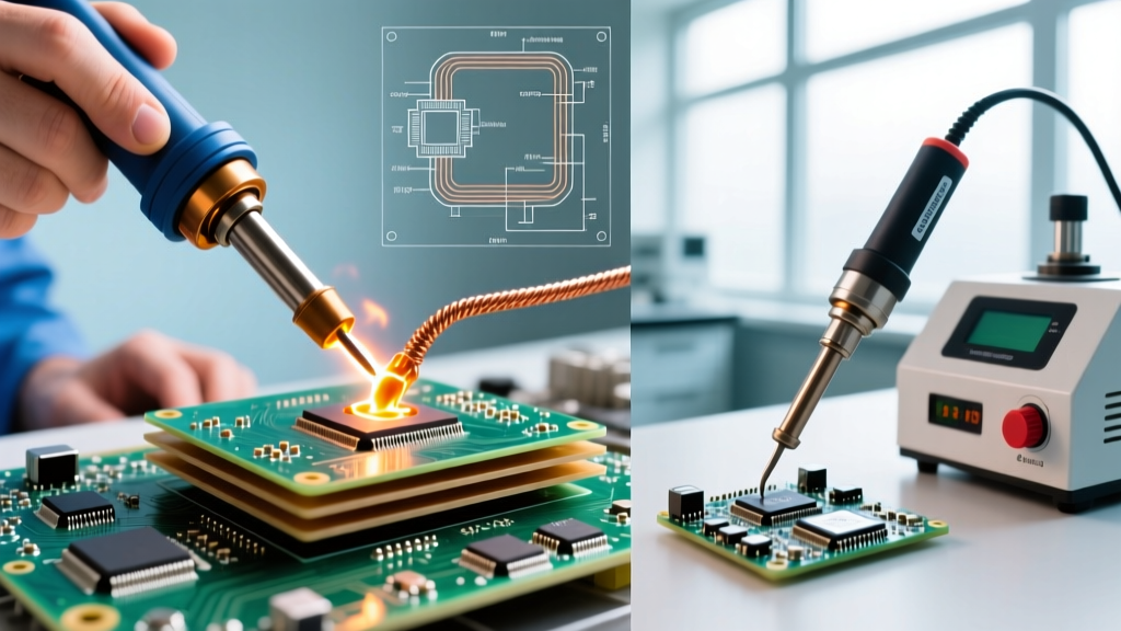
Components like QFNs (Quad Flat No-leads) and DFNs have thermal pads hidden beneath the chip. A soldering iron cannot reach these. You must use convective hot air. The Quick 861DW (approx. $260) offers the precise airflow and temperature stability required.
According to the NASA Workmanship Standards, proper convective heating requires maintaining a uniform thermal profile to prevent the 'popcorn effect' in moisture-sensitive ICs. Always bake moisture-sensitive components (MSL 3 or higher) at 125°C for 4-24 hours before hot air reflow.
Set your hot air station to 350°C with an airflow of 30-40%. Use a nozzle that is slightly larger than the IC footprint. Keep the handpiece moving in tight, continuous circles to avoid localized hot spots that can delaminate the PCB's FR4 substrate.
3. Reflow Soldering for Batch Production
If you are assembling 50 boards featuring dozens of 0402 passives and dense BGAs, hand soldering is economically unviable. Reflow soldering uses solder paste (a suspension of microscopic solder spheres in a volatile flux medium) and a controlled thermal profile.
For small-batch production in 2026, the T962A Reflow Oven (approx. $220) or a PID-controlled hotplate (like the Whizoo reflow controller paired with an induction cooktop) are excellent investments. The critical factor is following the alloy's specific thermal profile:
- Preheat Zone: Ramp to 150°C at 2°C/second to gently evaporate flux solvents without causing solder splatter.
- Soak Zone: Hold at 150°C - 175°C for 60-90 seconds to activate the rosin and equalize board temperature.
- Reflow Zone: Spike above the liquidus point (217°C for SAC305) for 45-60 seconds.
- Cooling Zone: Allow a natural, unforced cool down to form a fine-grain, mechanically strong crystalline structure.
Advanced Micro-Soldering and BGA Techniques
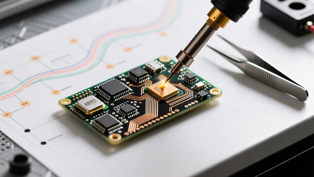
The proliferation of wearable tech and ultra-compact IoT nodes has pushed component sizes down to 01005 (0.4mm x 0.2mm). At this scale, human hands are no longer the limiting factor; vision and micro-motor control are. Micro-soldering requires a high-quality stereo zoom microscope (such as an AmScope 7X-45X trinocular setup, approx. $600) and a micro-pencil iron with a 0.1mm tip.
For Ball Grid Arrays (BGAs), the technique shifts from soldering to reballing. This involves applying a precise stencil of tacky flux (like Amtech NC-559-V2-TF), placing pre-formed SAC305 solder spheres, and using a specialized BGA rework station with top-and-bottom infrared heating to simultaneously reflow the spheres and attach the chip to the board.
The 2026 Soldering Technique Decision Tree
Use this step-by-step logical flow to finalize your technique selection for any new PCB design:
- Step 1: Identify the Minimum Pitch and Footprint.
If the smallest component is >0.5mm pitch and has exposed leads, default to Drag Soldering or Hand Soldering. If it is a bottom-terminated QFN or BGA, you must use Hot Air or Reflow. - Step 2: Calculate the Thermal Mass.
Are you soldering a heavy copper pour (e.g., 2oz or 3oz copper for power electronics)? If yes, manual techniques will fail due to heat sinking. You must employ a Bottom Pre-heater combined with a high-wattage iron (150W+ like the JBC CD-2BQE) or use Selective Wave Soldering. - Step 3: Evaluate Batch Volume.
For 1-10 prototypes, stick to manual iron and hot air. For 10-500 units, invest in a solder paste stencil and a Reflow Oven. For 500+ units, outsource to a PCBA house utilizing automated Wave and Selective Soldering machinery. - Step 4: Select the Alloy.
Consult the Indium Corporation Solder Alloy Guide to choose your metal. Use SAC305 for standard RoHS compliance, Sn63/Pb37 for legacy or high-reliability aerospace (where exempt), or low-temperature SnBiAg (melting point ~138°C) for heat-sensitive flexible PCBs and RF modules.
Real-World Failure Modes and Edge Cases
Even with the right technique chosen, execution errors lead to distinct failure modes. Recognizing these early saves hours of debugging.
- Tombstoning: Common in 0402 and 0201 reflow. Occurs when one pad heats faster than the other, causing the surface tension of the melting solder to pull the component upright. Fix: Ensure symmetrical trace routing to pads and use a slower ramp rate in the preheat zone.
- Cold Joints: Characterized by a dull, grainy, or lumpy appearance. Often caused by moving the component before the solder fully solidifies, or using an iron tip that is too small to transfer adequate heat to a ground plane. Fix: Increase thermal mass transfer (larger tip) and hold the component perfectly still for 3 seconds post-heat.
- Solder Bridging (Shorts): Highly prevalent in 0.5mm pitch drag soldering. Fix: You likely used too much solder and not enough flux. Apply additional liquid flux and use a clean, dry iron tip to wick away the excess, or use high-quality desoldering braid.
- Pad Lift / Delamination: The copper pad separates from the FR4 fiberglass. Fix: You applied heat for too long (exceeding 10 seconds per joint). Reduce iron temperature, use a more thermally efficient tip shape, or implement a board pre-heater.
Conclusion
Mastering modern electronics assembly is not about relying on a single tool; it is about applying the correct soldering techniques to the specific physical and thermal constraints of your PCB. By utilizing this decision framework, evaluating component geometries, and investing in the right thermal management tools, you can ensure robust, IPC-compliant solder joints whether you are building a single prototype or a small-batch production run.