
The Boot Sequence Minefield: Strapping Pins Explained
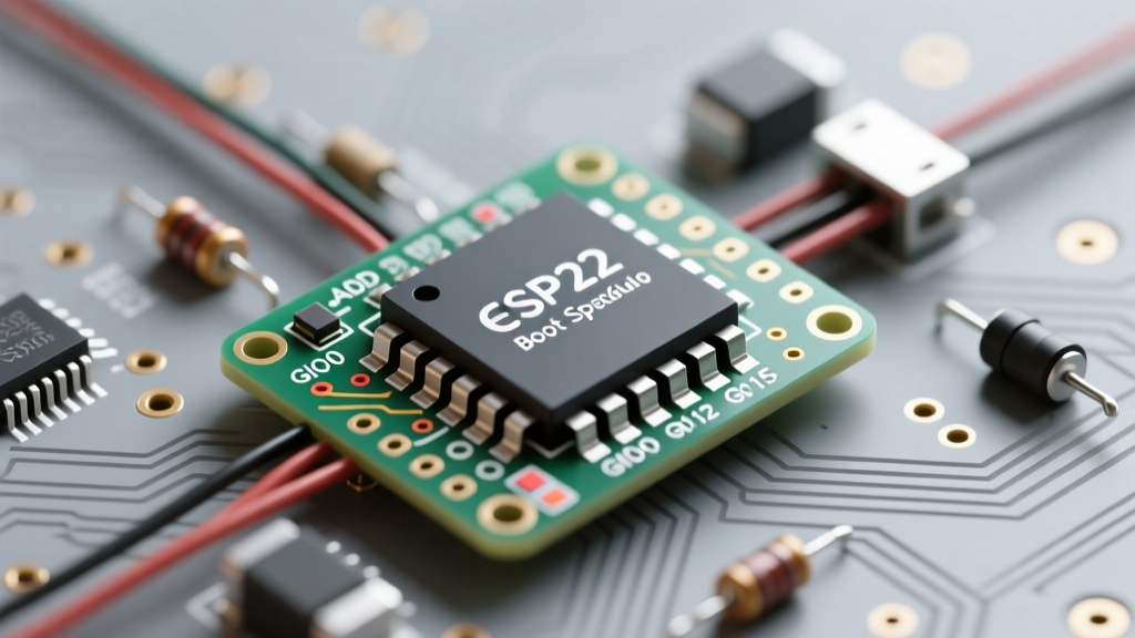
If you have spent any time in the ElectricalFlux forums, you know that 90% of ESP8266 project failures happen before a single line of code executes. The culprit? Strapping pins. The ESP8266 reads the logic levels of specific GPIOs during the first few milliseconds of power-on to determine its boot mode. If these pins are pulled to the wrong state by your sensors or relays, the microcontroller will silently hang or boot into an unintended SDIO mode.
Community veterans always warn newcomers about the "Big Three" strapping pins: GPIO0, GPIO2, and GPIO15. Here is the exact boot matrix that the official datasheet buries in the footnotes:
| Boot Mode | GPIO15 (MTDO) | GPIO0 | GPIO2 | Common Community Use Case |
|---|---|---|---|---|
| Flash Boot (Normal) | LOW | HIGH | HIGH | Running your Arduino/ESPHome sketch |
| UART Download (Flash) | LOW | LOW | HIGH | Uploading code via USB/Serial |
| SDIO Boot | HIGH | X | X | Rarely used; usually an accidental trap |
"Never wire a relay directly to GPIO15 or GPIO2. If the relay defaults to a HIGH or LOW state that conflicts with the boot matrix, your ESP8266 becomes a brick until you disconnect the wire." — ElectricalFlux Community Moderator
Universal ESP8266 Pinout Mapping Table
The silkscreen on development boards is notoriously confusing. NodeMCU uses "D" numbering (e.g., D4), while the raw ESP-12F chip uses GPIO numbering (e.g., GPIO2). The Wemos D1 Mini maps these slightly differently in physical layout, though the internal GPIO mapping remains identical. Below is the definitive cross-reference table maintained by our community.
| NodeMCU Silk | Wemos D1 Silk | Raw ESP-12F GPIO | Voltage Tolerance | Safe for Boot? | Primary Function / Quirks |
|---|---|---|---|---|---|
| D0 | - | GPIO16 | 3.3V | Yes | Deep Sleep Wake (No PWM/Interrupts) |
| D1 | D1 | GPIO5 | 3.3V | Yes | Default I2C SCL |
| D2 | D2 | GPIO4 | 3.3V | Yes | Default I2C SDA |
| D3 | D3 | GPIO0 | 3.3V | NO | Flash Button (Must be HIGH on boot) |
| D4 | D4 | GPIO2 | 3.3V | NO | Onboard LED (Must be HIGH on boot) |
| D5 | D5 | GPIO14 | 3.3V | Yes | Default SPI SCK |
| D6 | D6 | GPIO12 | 3.3V | Yes | Default SPI MISO |
| D7 | D7 | GPIO13 | 3.3V | Yes | Default SPI MOSI / Boot TX2 |
| D8 | D8 | GPIO15 | 3.3V | NO | Default SPI CS (Must be LOW on boot) |
| RX | RX | GPIO3 | 3.3V | Yes | Hardware UART RX |
| TX | TX | GPIO1 | 3.3V | Yes | Hardware UART TX (Debug log on boot) |
| A0 | A0 | ADC (TOUT) | 1.0V Max | Yes | Analog Input (0-1V range only) |
Hardware Quirks the Datasheet Buries
When designing custom PCBs or wiring complex sensor arrays, the community has documented several hardware limitations that routinely trip up makers transitioning from the Arduino Uno or Nano ecosystem.
The 1-Volt ADC Trap
Unlike the ATmega328P on the Arduino Uno, which features a 0-5V ADC, the ESP8266's internal Analog-to-Digital Converter (ADC) on the TOUT pin maxes out at 1.0 Volts. Applying 3.3V to the A0 pin will not yield a maximum reading; it will saturate the ADC and potentially degrade the silicon over time.
Community Solution: If you need to measure a LiPo battery voltage (up to 4.2V) or a 3.3V logic signal, you must build a voltage divider. The most reliable community-tested resistor combination is a 220kΩ and 100kΩ resistor pair. This scales a 4.2V input down to roughly 1.3V (which slightly exceeds the 1V limit, so a 330k/100k is safer for LiPo). Always buffer the ADC with a 100nF ceramic capacitor to ground to reduce Wi-Fi RF noise jitter.
GPIO16 (D0): The Odd One Out
GPIO16 is physically located at the bottom right of the ESP-12F module. It is tied to the Real-Time Clock (RTC) and is the only pin capable of waking the ESP8266 from Deep Sleep. To use Deep Sleep, you must physically wire D0 to the RST pin. However, the trade-off is severe: GPIO16 does not support hardware PWM, cannot trigger external interrupts, and does not have an internal pull-up resistor. Do not use D0 for button inputs or servo control.
Community Wiring Standards for I2C and SPI
While the ESP8266 allows software-defined I2C and SPI on almost any pin via the Arduino Wire and SPI libraries, the community strongly recommends adhering to the hardware-default pins to avoid boot conflicts and leverage internal routing optimizations.
- I2C Defaults: SDA on D2 (GPIO4) and SCL on D1 (GPIO5). These pins are safe during boot and feature internal pull-up resistors (though external 4.7kΩ pull-ups are still recommended for long wire runs or high-speed sensors like the BME280).
- SPI Defaults: SCK on D5 (GPIO14), MISO on D6 (GPIO12), MOSI on D7 (GPIO13), and CS on D8 (GPIO15). Warning: Because GPIO15 (D8) must be LOW on boot, your SPI slave device (like an SD card module) must not pull the CS line HIGH during power-on. If it does, the ESP8266 will fail to boot. Use a different GPIO for CS if your slave device has an active pull-up.
Power Delivery and RF Spikes
A frequent topic of debate in our DIY forums revolves around power brownouts. The ESP8266 is a Wi-Fi transceiver; when it transmits data, it can draw current spikes exceeding 350mA for microseconds. If you are using a bare ESP-12F module on a breadboard, the long jumper wires introduce inductance and resistance, causing the VCC rail to droop below the 2.5V brownout threshold, triggering a spontaneous reboot.
According to the official Espressif Hardware Design Guidelines, you must place a 10µF to 100µF tantalum or ceramic capacitor as close to the VCC and GND pins of the ESP-12F as physically possible. For NodeMCU and Wemos D1 Mini boards, the onboard AMS1117-3.3 LDO usually handles these spikes adequately, provided your USB cable is of high quality and can supply at least 1A continuously.
Essential Resources & Further Reading
To continue mastering the ESP8266 ecosystem, we recommend bookmarking the following community-trusted resources:
- Random Nerd Tutorials: ESP8266 Pinout Reference - Excellent visual diagrams for NodeMCU and Wemos D1 Mini silkscreens.
- NodeMCU Official Documentation - Deep dive into Lua and C++ GPIO manipulation, interrupt handling, and deep sleep architecture.
- Espressif ESP8266 Hardware Design Guidelines - The definitive PDF for custom PCB layout, antenna clearance, and strapping pin circuitry.
By respecting the strapping pins, managing the 1V ADC limit, and providing clean power, your ESP8266 projects will transition from frustrating breadboard experiments to reliable, long-term IoT deployments.