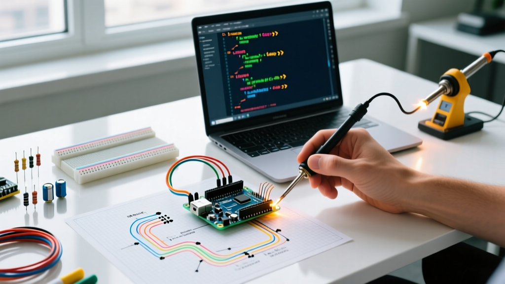

Transitioning from Breadboards to Custom PCBs
Moving from a breadboard prototype to a manufactured printed circuit board (PCB) is a major milestone for any maker or embedded engineer. To bridge this gap, you need a reliable Arduino schematic diagram maker that allows you to translate your physical wiring into a precise, manufacturable electronic schematic. Whether you are designing a low-power IoT sensor node using an ATmega328P or a complex motor controller, mastering schematic capture is non-negotiable.
In this comprehensive 2026 tutorial, we will explore the best schematic tools available, compare their ecosystems, and walk through a step-by-step guide to designing a standalone Arduino-compatible microcontroller board from scratch. We will focus on professional-grade practices, including proper decoupling, auto-reset circuitry, and crystal load capacitance calculations.
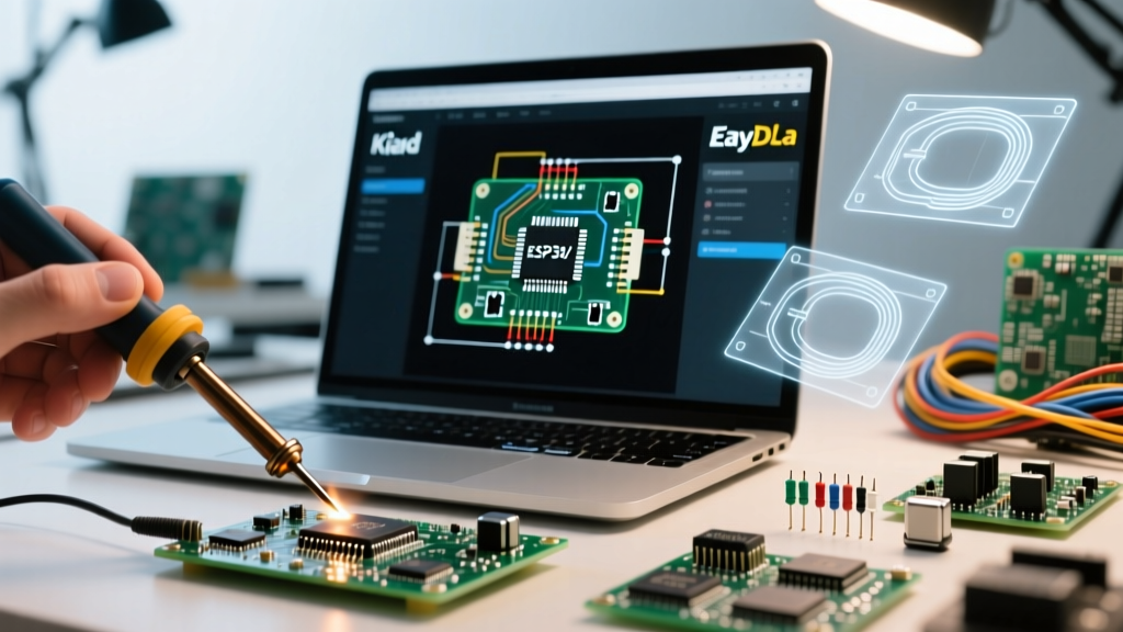
Comparing the Top 3 Arduino Schematic Diagram Makers
Before placing your first component symbol, you must choose the right electronic design automation (EDA) software. The landscape has evolved significantly, with cloud-based and open-source tools dominating the maker space.
| Tool | Pricing (2026) | Library Ecosystem | Best Use Case |
|---|---|---|---|
| KiCad 9.x | Free / Open Source | Massive (SnapEDA, Ultra Librarian, GitHub) | Professional, complex, multi-layer boards |
| EasyEDA Pro | Free (Std) / $99/yr (Pro) | Direct LCSC integration (200k+ parts) | Rapid prototyping and direct JLCPCB ordering |
| Fritzing | $24 (One-time) | Limited, mostly basic maker modules | Beginners, educational visual documentation |
For this tutorial, we will use KiCad EDA Suite. It is the industry standard for open-source hardware design, offering a fully unrestricted schematic capture and PCB layout environment without artificial pin-count limits or paywalls.
Step-by-Step Tutorial: Designing an ATmega328P Standalone Board
We will design a custom board based on the ATmega328P-AU (the surface-mount TQFP-32 version, which costs roughly $1.80 in low volumes compared to the $3.50+ DIP version). This design will include a USB-to-UART bridge and an auto-reset circuit so it can be programmed directly via the Arduino IDE.
Step 1: Setting Up the Schematic Environment
Open KiCad and create a new project. The first critical step is ensuring you have high-quality, verified footprint libraries. Do not rely solely on the default libraries for specialized maker components.
- Navigate to the SparkFun KiCad Libraries on GitHub and clone the repository to your local machine.
- In KiCad, go to Preferences > Manage Symbol Libraries and add the SparkFun `.kicad_sym` files as global libraries.
- Repeat this process in the Manage Footprint Libraries menu for the `.pretty` folders.
This guarantees that when you place a component like the CH340C USB-UART bridge, the schematic symbol perfectly matches the physical SMD footprint (SOP-16) on the PCB.
Step 2: Placing the Core Microcontroller and Decoupling
Place the ATmega328P-AU symbol in the center of your workspace. The most common failure mode in custom Arduino designs is inadequate power decoupling, leading to erratic brownouts and ADC noise.
According to the Microchip ATmega328P Product Page and datasheet, you must place decoupling capacitors as close to the power pins as physically possible in the PCB layout phase. In the schematic phase, wire the following:
- VCC (Pins 7, 20) and AVCC (Pin 22): Connect a 100nF (0.1µF) X7R ceramic capacitor from each pin to GND.
- AREF (Pin 20): If using the internal ADC reference, place a 100nF capacitor to GND to filter high-frequency noise. Do not connect an external voltage to AREF if you plan to use the internal 1.1V or 5V references in your sketch.
- Clock Source: Place a 16MHz quartz crystal (HC49 or 3225 SMD package) on pins 9 (XTAL1) and 10 (XTAL2).
Expert Tip: Crystal Load Capacitance Math
Do not blindly use 22pF capacitors for your crystal. You must calculate the exact load capacitance ($C_L$) using the formula: $C_L = \frac{C_1 \cdot C_2}{C_1 + C_2} + C_{stray}$. If your 16MHz crystal specifies a 18pF load, and your PCB stray capacitance ($C_{stray}$) is estimated at 3pF, you need 30pF capacitors for $C_1$ and $C_2$. Always use C0G/NP0 dielectric capacitors for timing circuits, as X7R capacitors exhibit capacitance drift with temperature and voltage.
Step 3: Adding the Auto-Reset Circuit (The FTDI Trick)
To upload sketches via the Arduino IDE without manually pressing a reset button, you must replicate the auto-reset circuit found on the Arduino Uno R3.
- Place a 10kΩ pull-up resistor from the RESET pin (Pin 29 / PC6) to VCC (5V).
- Place a 100nF ceramic capacitor in series between the DTR (Data Terminal Ready) line of your USB-UART bridge and the RESET pin.
How it works: When the Arduino IDE initiates an upload, the USB-UART bridge pulls the DTR line LOW. The 100nF capacitor acts as a differentiator, creating a momentary voltage drop on the RESET pin, pulling it below the logic LOW threshold just long enough to trigger the bootloader. If you omit this capacitor, you will be forced to manually press a physical reset button the exact millisecond the IDE finishes compiling.
Step 4: Power Regulation and USB Interfacing
For USB connectivity, you have two primary choices in 2026:
- CH340C: Extremely cost-effective ($0.30 in bulk). Requires an external 12MHz crystal and two 47pF load capacitors. Highly reliable but takes up more PCB real estate.
- CP2102N: More expensive ($1.50+), but features an internal oscillator, eliminating the need for an external crystal. Available in a compact QFN-28 package.
If your board will be powered by an external 9V battery or a 12V wall adapter, you must include a voltage regulator. The classic AMS1117-5.0 LDO is a popular choice, but be aware of its dropout voltage (typically 1.1V). To get a stable 5.0V output, your input voltage must be at least 6.1V. Furthermore, the AMS1117 can dissipate significant heat; if you are drawing 200mA from a 12V source, the regulator will dissipate $(12V - 5V) \times 0.2A = 1.4W$ of heat. Ensure your PCB layout includes adequate thermal vias and copper pours under the SOT-223 tab.
Common Schematic Capture Pitfalls and How to Avoid Them
Even experienced engineers make mistakes during schematic capture. Run through this checklist before generating your netlist:
- Missing I2C Pull-ups: The ATmega328P internal pull-ups (20kΩ - 50kΩ) are too weak for reliable I2C communication at 400kHz. Always add external 4.7kΩ pull-up resistors to SDA (A4) and SCL (A5) if you are connecting sensors like the BME280 or MPU6050.
- Unused Input Pins: Leaving CMOS input pins floating can cause them to oscillate linearly, drawing excessive current and generating EMI noise. Tie unused pins to GND via a 10kΩ resistor or configure them as outputs in your firmware.
- Incorrect Power Flags: KiCad requires explicit power flags (like `+5V` and `GND`) to understand where power originates. If you don't use the `PWR_FLAG` symbol on your voltage regulator output, the Electrical Rules Check (ERC) will throw an error warning that your 5V rail is undriven.
Exporting to PCB Layout and Design Rule Checks
Once your schematic is complete, run the Electrical Rules Checker (ERC). Fix all errors (red bugs) and review all warnings (yellow triangles). Pay special attention to unconnected pins and power flag conflicts.
When transitioning to the PCB layout editor, keep these 2026 manufacturing standards in mind for standard 2-layer FR4 boards (1.6mm thickness, 1oz copper):
- Trace Widths: Use 10mil (0.25mm) traces for signal lines (capable of ~0.5A). For the main 5V and GND rails, use at least 30mil to 40mil traces to handle higher current loads and reduce voltage drop.
- Clearances: Set your minimum clearance to 6mil (0.15mm). Most modern PCB fabs like JLCPCB and PCBWay handle 6mil effortlessly without upcharging.
- Vias: Standard 0.3mm drill / 0.6mm pad vias are reliable and cheap. Avoid microvias unless you are designing a 4+ layer high-density board.
Final Thoughts on Schematic Workflows
Mastering an Arduino schematic diagram maker is about more than just connecting dots on a screen; it is about understanding the electrical realities of the components you are specifying. By carefully calculating load capacitances, implementing proper decoupling strategies, and designing robust auto-reset circuits, you ensure that your custom PCB will boot up and accept code on the very first manufacture run. Take the time to verify your footprints against the physical datasheets, and your transition from breadboard to custom silicon will be seamless.