
The Foundation of the Arduino Ecosystem: Understanding the Uno R3 Pinout
Even as we navigate through 2026 with advanced AI-accelerated microcontrollers and high-speed ESP32-S3 variants, the Arduino Uno R3 remains the undisputed anchor of the DIY electronics ecosystem. At its core lies the Microchip ATmega328P-PU, an 8-bit AVR microcontroller that has defined physical computing for over a decade. However, successfully integrating sensors, motor drivers, and stacked shields requires more than just memorizing pin numbers. It demands a deep, electrical-level understanding of the Arduino Uno R3 pinout, its hardware timer conflicts, power delivery limitations, and the specific R3 header revisions that dictate shield compatibility.
This comprehensive ecosystem overview dissects the Uno R3 pinout, moving beyond basic tutorials to expose the real-world edge cases, thermal constraints, and architectural quirks that professional engineers and advanced makers must navigate.
Power Architecture: Beyond the 5V and 3.3V Labels
The power header on the Uno R3 consists of six pins, but treating them as simple voltage taps is a primary cause of hardware failure in complex ecosystems. According to the official Arduino Uno R3 documentation, the board features two distinct voltage regulation stages.
The 5V Rail and VIN Constraints
The VIN pin accepts unregulated input voltage, which is then stepped down to 5V by an NCP1117ST50T3G linear regulator. While the absolute maximum input is 20V, the recommended operating window is 7V to 12V. Pushing 12V through the VIN pin while drawing 200mA from the 5V rail forces the linear regulator to dissipate roughly 1.4 Watts of heat. Without active cooling, the onboard thermal shutdown will trigger, causing erratic microcontroller resets.
Expert Warning: If your ecosystem includes high-draw components like servo motors or LED matrices, bypass the onboard regulator entirely. Supply a regulated 5V source directly to the 5V pin, completely ignoring the VIN and barrel jack. The 5V pin is directly tied to the ATmega328P's VCC rail and can safely handle up to 800mA, limited only by your external power supply and the PCB trace width.
The 3.3V Pin: A Legacy Misconception
On older FTDI-based Arduino boards, the 3.3V pin was limited to a meager 50mA, sourced directly from the USB-serial converter chip. The Uno R3 upgraded this architecture. It utilizes a dedicated NCP1117 3.3V LDO capable of sourcing up to 150mA. This is sufficient for powering low-energy ecosystem additions like LoRa modules (e.g., RFM95W in sleep/listen modes) or I2C environmental sensors, but it will brownout if used to drive high-power WiFi transceivers without an external buck converter.
Digital I/O, PWM Timers, and Interrupt Mapping
The Uno R3 exposes 14 digital I/O pins (D0-D13). Six of these are hardware PWM capable (marked with a tilde ~), and two are tied to external hardware interrupts. Understanding the underlying ATmega328P timer architecture is critical when integrating audio, motor control, or RF libraries into your project.
The Timer Conflict Matrix
The ATmega328P utilizes three hardware timers to generate PWM signals and manage internal clock functions. Modifying the PWM frequency on specific pins will inadvertently break core Arduino functions.
- Pins 5 & 6 (Timer0): Operate at ~980 Hz by default. Critical Ecosystem Note: Timer0 is hardcoded to manage the
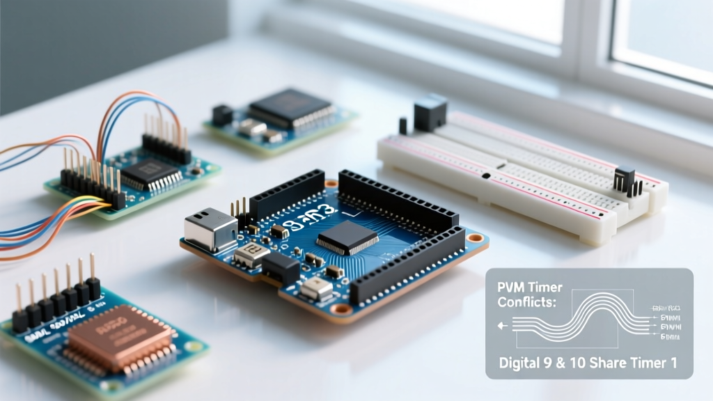
millis(),delay(), andmicros()functions. Altering the prescaler on Timer0 for custom motor control frequencies will completely destroy your timing logic. - Pins 9 & 10 (Timer1): Operate at ~490 Hz. This is a 16-bit timer, offering high-resolution PWM ideal for precision servo control and audio synthesis.
- Pins 3 & 11 (Timer2): Operate at ~490 Hz. Timer2 is frequently hijacked by ecosystem libraries like
Tone.hfor buzzer generation or by software-based RF24 network stacks.
Hardware Interrupts (INT0 and INT1)
Pins D2 and D3 are mapped to hardware interrupts. In an ecosystem relying on rotary encoders, flow meters, or anemometers, routing signals to D2/D3 ensures zero-latency pulse counting without relying on the slower, polling-based digitalRead() function inside the main loop.
Communication Buses: I2C, SPI, and UART
Integrating modular shields requires strict adherence to the Uno R3's communication bus routing. For a deeper dive into bus protocols, the SparkFun SPI Tutorial provides excellent electrical context.
I2C and the R3 Header Revision
Historically, I2C was exclusively mapped to Analog pins A4 (SDA) and A5 (SCL). The defining feature of the 'R3' revision was the addition of dedicated SDA and SCL pins on the digital header block, placed adjacent to the AREF pin. This was a massive ecosystem shift: it allowed shield designers to route I2C lines without consuming analog inputs, and it standardized physical pin locations across 5V (Uno) and 3.3V (Due/Zero) boards.
When stacking multiple I2C shields, be mindful of pull-up resistor capacitance. Each shield typically includes 4.7kΩ pull-up resistors to 5V. Stacking four shields places four sets of resistors in parallel (yielding ~1.17kΩ) and adds significant bus capacitance, which can corrupt data packets at 400 kHz Fast Mode. If your I2C bus fails, consult the NXP I2C-bus specification to calculate your maximum allowable capacitance and remove redundant pull-ups.
SPI and UART
- SPI (D10-D13): Used for high-speed peripherals like SD card modules, TFT displays, and CAN bus transceivers. D10 (SS), D11 (MOSI), D12 (MISO), D13 (SCK).
- UART (D0-D1): Hardware serial (RX/TX). Because these pins are hardwired to the ATmega16U2 USB-to-Serial bridge, connecting high-impedance sensors here will interfere with code uploading. Always use
SoftwareSerialon alternative pins if your ecosystem requires multiple UART devices.
Comprehensive Pinout & Ecosystem Mapping Table
| Pin | Primary Function | Ecosystem Use Case | Hardware Conflict / Note |
|---|---|---|---|
| D0 (RX) | UART Receive | GPS Modules, Bluetooth HC-05 | Conflicts with USB Serial upload |
| D2 | INT0 | Rotary Encoders, Interrupt Sensors | Required for hardware interrupt 0 |
| D3 (~) | PWM / INT1 | LED Dimming, Servo Control | Shares Timer2 with Tone library |
| D10 (~) | SPI SS / PWM | SD Cards, Ethernet Shields | Must remain HIGH to disable SPI slaves |
| D11 (~) | SPI MOSI | TFT Displays, RF24 Radios | Cannot be used for PWM when SPI is active |
| D13 | SPI SCK / LED | Onboard Status, SPI Clock | Onboard LED circuit adds slight capacitance |
| A4 | ADC4 / I2C SDA | OLED Displays, IMUs (MPU6050) | Duplicated on R3 dedicated I2C header |
| A5 | ADC5 / I2C SCL | Environmental Sensors (BME280) | Duplicated on R3 dedicated I2C header |
Shield Compatibility and the IOREF Standard
The physical layout of the Arduino Uno R3 pinout introduced the IOREF pin. This was a masterstroke for ecosystem longevity. IOREF outputs the operating voltage of the microcontroller (5V on the Uno R3). Advanced 3.3V ecosystem shields (like those designed for the Arduino Zero or Due) read the IOREF pin via an onboard comparator or level-shifter IC (such as the TXB0104). If the shield detects 5V on IOREF, it automatically activates bi-directional logic level shifters to protect its sensitive 3.3V silicon. When designing custom PCB shields for the Uno R3 ecosystem in 2026, routing the IOREF pin to your logic enable circuits is considered mandatory best practice.
The 'Unconnected' Pin Mystery
Next to IOREF, the R3 revision added a fourth pin in the bottom left header block that is intentionally left unconnected (NC) on the Uno R3. This pin was reserved for future use and is tied to the RESET pin on newer, specialized derivatives. Shield designers must leave this pin floating to ensure backward and forward compatibility across the entire Arduino ecosystem.
Real-World Edge Cases in Ecosystem Integration
When stacking multiple shields to build complex IoT gateways or robotics controllers, physical and electrical edge cases emerge:
- Physical Clearance: Standard female headers are 8.5mm tall. When stacking an Ethernet shield beneath a motor driver shield, the RJ45 jack or USB port will short against the bottom of the top shield. Always use 10.5mm or 11mm stacking headers for multi-shield ecosystems.
- ADC Crosstalk: The ATmega328P's ADC uses a sample-and-hold capacitor. If you read a high-impedance analog sensor on A0 and immediately read a low-impedance sensor on A1, the residual charge can skew the A1 reading. Insert a dummy
analogRead()on the target pin and discard the result before taking your actual measurement to allow the internal capacitor to settle. - Reset Capacitor Hack: In permanent installations where auto-reset via serial DTR is undesirable (causing the board to reboot when a PC connects for logging), placing a 10µF electrolytic capacitor between the RESET and GND pins will absorb the DTR pulse, locking the board in run-mode.
Conclusion
Mastering the Arduino Uno R3 pinout is about understanding the electrical realities beneath the silkscreen. By respecting the thermal limits of the NCP1117 regulators, avoiding Timer0 for custom PWM, managing I2C bus capacitance, and leveraging the IOREF standard, you can build robust, multi-shield ecosystems that operate flawlessly in real-world conditions. Whether you are prototyping a 2026 smart-agriculture node or maintaining legacy industrial automation hardware, the Uno R3 remains a masterclass in accessible, extensible hardware design.