
The Arduino Uno pin configuration is the foundational blueprint of the modern open-source hardware ecosystem. Since its inception, the physical footprint and header layout of the Uno have dictated the design of thousands of third-party shields, sensor breakout boards, and robotics chassis. However, as the platform has evolved from the classic ATmega328P-based Uno R3 to the modern Renesas-powered Uno R4 Minima and R4 WiFi, the electrical realities behind those familiar 0.1-inch pitch headers have shifted significantly.
For hardware engineers, DIY enthusiasts, and educators designing for the Arduino ecosystem in 2026, understanding the nuances of the Arduino Uno pinout is no longer just about memorizing digital and analog pin numbers. It requires a deep understanding of logic level tolerances, PWM frequency routing, ADC resolutions, and backward-compatibility edge cases. This ecosystem overview dissects the Uno pin configuration, contrasting the legacy R3 architecture with the modern R4 series to ensure your shields and wiring harnesses function flawlessly across the entire product line.
The Evolution of the Arduino Uno Pinout
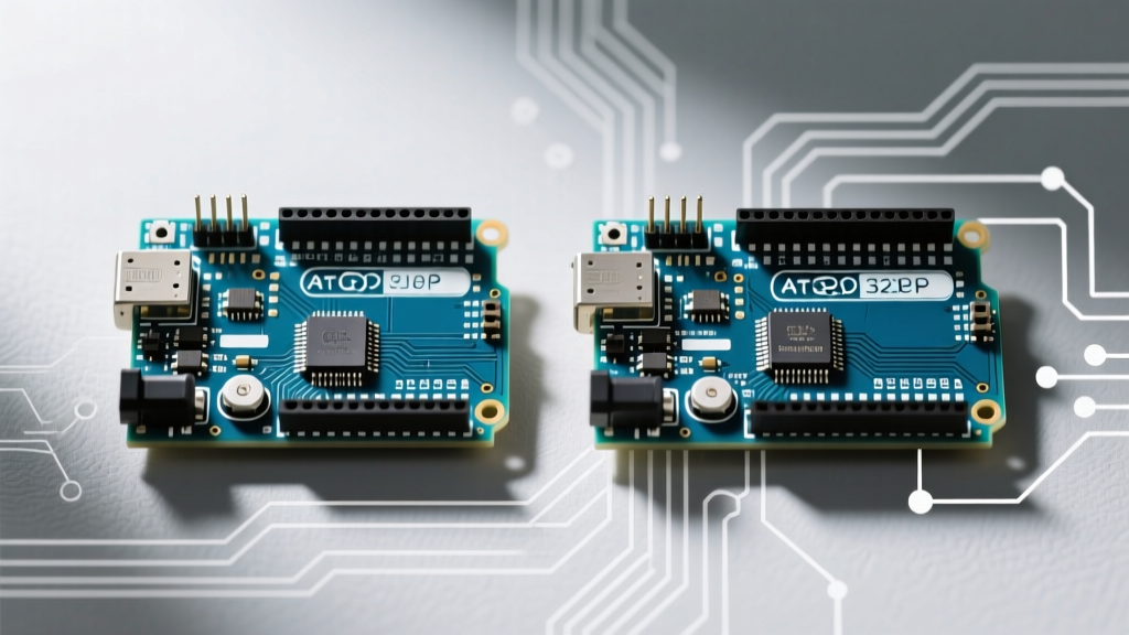
While the physical dimensions of the Uno board (2.1" x 2.7") and the placement of the 14-pin and 10-pin headers have remained strictly identical to maintain mechanical shield compatibility, the silicon driving the pins has undergone a massive generational leap. The transition from the 8-bit AVR architecture to the 32-bit Arm Cortex-M4 (and the addition of an ESP32-S3 coprocessor on the WiFi model) has expanded the electrical capabilities of the pinout.
Hardware Compatibility Matrix: R3 vs. R4 Series
Before wiring complex sensor arrays or designing custom PCB shields, review the architectural differences that affect how the Arduino Uno pin configuration behaves under the hood.
| Feature | Uno R3 (Legacy) | Uno R4 Minima | Uno R4 WiFi |
|---|---|---|---|
| Core MCU | ATmega328P (8-bit AVR) | Renesas RA4M1 (Arm Cortex-M4) | RA4M1 + ESP32-S3 Coprocessor |
| Typical Retail Price | $27.00 | $19.99 | $27.50 |
| Digital I/O Pins | 14 | 14 | 14 |
| PWM Capable Pins | 6 (Pins 3, 5, 6, 9, 10, 11) | 14 (All digital pins) | 14 (All digital pins) |
| Analog Inputs | 6 (10-bit ADC) | 6 (12-bit ADC, 14-bit capable) | 6 (12-bit ADC, 14-bit capable) |
| DAC Output | None (PWM only) | 1 (True 12-bit DAC on A0) | 1 (True 12-bit DAC on A0) |
| Native Logic Level | 5V | 5V Tolerant I/O | 5V Tolerant I/O |
Decoding the Arduino Uno Pin Configuration
To effectively integrate the Uno into a broader sensor or actuator ecosystem, we must break down the specific electrical characteristics of the three primary header blocks: Power, Digital/PWM, and Analog/Communication.
Power Delivery and Voltage Tolerances
The power header remains the most critical point of failure in custom ecosystem designs. The 5V pin bypasses the onboard voltage regulator and connects directly to the USB 5V rail (when powered via USB) or the regulator output (when powered via the barrel jack/VIN).
- The 3.3V Pin Shift: On the classic Uno R3, the 3.3V pin is sourced from the secondary regulator on the USB-to-Serial ATmega16U2 chip, limiting its current capacity to a meager 50mA. On the Uno R4 series, the 3.3V rail is driven by a dedicated, robust buck converter capable of sourcing up to 150mA. This is a massive advantage for powering modern 3.3V I2C sensors and low-power LoRa modules directly from the shield header.
- VIN and the Polyfuse: The VIN pin accepts 7V to 12V (recommended). However, USB-powered designs must remember the resettable PTC polyfuse on the USB line, which trips at 500mA. If your shield draws heavy current (e.g., driving multiple 5V relays or a high-torque servo), you must bypass the USB and supply power directly through the barrel jack or VIN pin.
Digital I/O, PWM Routing, and the DAC Shift
The digital header provides 14 general-purpose I/O pins. However, how these pins handle pulse-width modulation (PWM) and analog output varies drastically between generations.
On the Uno R3, only six pins (marked with a tilde '~') support hardware PWM, operating at fixed frequencies of 490 Hz or 980 Hz. The R4 series utilizes the RA4M1's advanced timer peripherals, enabling hardware PWM on all 14 digital pins with customizable frequencies up to 65 kHz. This makes the R4 vastly superior for driving brushless DC (BLDC) motor controllers or high-frequency switching power supplies via custom shields.
Expert Warning: The A0 DAC Edge Case
On the Uno R4 Minima and WiFi, pin A0 doubles as a true 12-bit Digital-to-Analog Converter (DAC). Unlike the digital I/O pins which output 5V logic levels for backward compatibility, the DAC on A0 outputs a maximum of 3.3V. If you are designing an audio shield or an analog control voltage (CV) module for synthesizers, you must account for this 3.3V ceiling or implement an op-amp gain stage on your shield PCB.
Communication Protocols: UART, I2C, and SPI
The ecosystem relies heavily on standardized communication buses. The Arduino Uno pin configuration maps these as follows:
- UART (Serial): Mapped to pins 0 (RX) and 1 (TX). On the R3, these are tied directly to the ATmega16U2 USB bridge. On the R4 WiFi, an additional hardware UART is available via the ESP32-S3 coprocessor, but routing it requires specific firmware bridging.
- I2C (Wire): Mapped to A4 (SDA) and A5 (SCL), as well as the dedicated 4-pin header near the USB port.
- SPI: Mapped to pins 11 (MOSI), 12 (MISO), and 13 (SCK). The Chip Select (CS) pin is user-defined, but standard ecosystem shields (like the Ethernet Shield or MicroSD module) default to pin 10 or pin 4.
Shield Compatibility: Physical vs. Electrical Integration
The physical footprint of the Uno is sacred in the maker community. The 2.54mm (0.1") pitch headers, the 1.6" offset between the digital and analog rows, and the specific placement of the mounting holes ensure that a shield designed in 2012 will physically mate with an Uno R4 WiFi today. However, electrical compatibility requires deeper scrutiny.
The I2C Pull-Up Resistor Conflict
One of the most common failure modes when migrating legacy shields to modern boards involves the I2C bus. The classic Uno R3 features 10kΩ physical pull-up resistors on the SDA and SCL lines, tied to 5V. Many older 5V shields (like early LCD displays or the BMP180 barometric sensor) rely on these onboard pull-ups and omit their own.
The Uno R4 series handles I2C differently, often relying on internal MCU pull-ups or different routing to accommodate the 5V-tolerant open-drain architecture of the RA4M1. If you connect a legacy shield lacking its own pull-ups to an R4, you may experience I2C ACK failures or bus lockups. The Fix: Always design custom shields with dedicated 4.7kΩ pull-up resistors on the SDA/SCL lines, jumpered to the appropriate logic voltage, rather than relying on the host board's internal configuration.
Real-World Failure Modes and Edge Cases
When integrating the Uno into complex DIY ecosystems, keep an eye out for these specific hardware edge cases:
- SPI Speed Limitations: The ATmega328P on the R3 maxes out its SPI clock at half the system clock (8 MHz). The RA4M1 on the R4 can push SPI speeds significantly higher. If you are using a level-shifting shield with slow MOSFETs (like the BSS138) designed for 8 MHz, pushing the R4 SPI bus to 20 MHz will result in signal degradation and corrupted data on TFT displays or external flash memory.
- Analog Reference (AREF) Vulnerabilities: The AREF pin allows you to set a custom voltage reference for the ADC. On the R3, applying a voltage higher than 5V or feeding current into the AREF pin without calling
analogReference(EXTERNAL)in software can permanently short the internal AVCC rail. The R4 includes better internal protection, but best practice dictates always using a 100Ω series resistor on the AREF line when connecting external precision voltage references. - PWM Resolution Defaults: While the R4 hardware supports up to 12-bit PWM resolution, the Arduino core defaults to 8-bit (0-255) to maintain backward compatibility with R3 code. If your motor control shield requires fine-grained 12-bit resolution, you must explicitly reconfigure the timer registers in your setup loop.
Frequently Asked Questions (FAQ)
Can I use 3.3V sensors with the 5V Arduino Uno R3?
Not directly on the I/O pins. The Uno R3 outputs 5V on its digital pins, which will fry the GPIO of a strict 3.3V sensor (like the BME280 or nRF24L01). You must use a bidirectional logic level shifter or a voltage divider on the MOSI/SCL lines. Conversely, the Uno R4 is natively 5V tolerant on its inputs, making 3.3V sensor integration much safer, provided you respect the 3.3V output limits of the sensor's TX/SDA lines.
Why do some shields use pins A4 and A5 for I2C if there is a dedicated header?
Legacy shields designed before 2014 (pre-Uno R3 revision) map I2C exclusively to A4 and A5. The dedicated I2C header was added in the R3 revision to accommodate the larger ATmega16U2 USB chip footprint and to ensure I2C availability on boards like the Mega, where A4/A5 do not map to the hardware I2C bus. Modern shield designs should route I2C to the dedicated 4-pin header near the USB port for cross-board ecosystem compatibility.
Does the ESP32-S3 on the Uno R4 WiFi interfere with the digital pins?
The ESP32-S3 acts as a network coprocessor and communicates with the main RA4M1 via an internal SPI bus. It does not hijack the external digital header pins (0-13) for its own Wi-Fi/Bluetooth operations. However, the SWD (Serial Wire Debug) pins and specific test pads on the underside of the R4 WiFi board are tied to the ESP32-S3 for firmware updates, which is a crucial detail if you are designing a custom baseplate or enclosure with pogo-pin contacts.