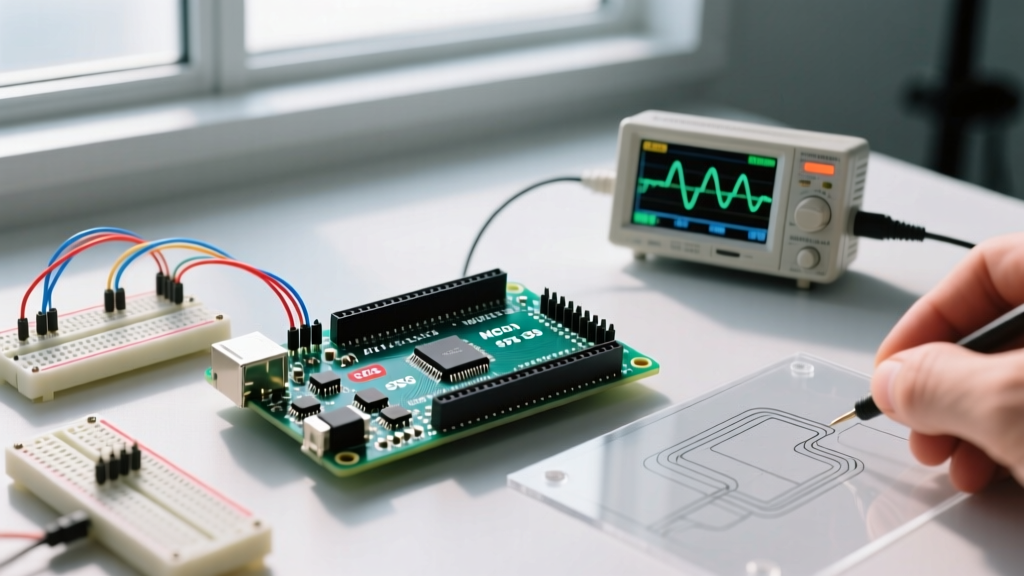

Introduction to ATmega2560 SPI Performance
Understanding the exact arduino mega spi pinout is only the first step in building high-speed peripheral interfaces. While many tutorials stop at identifying which wires go where, professional embedded engineers know that physical pin mapping is merely the baseline. The real challenge lies in pushing the Serial Peripheral Interface (SPI) to its theoretical limits without triggering data corruption, timing violations, or ground bounce. In this comprehensive benchmark guide, we evaluate the true throughput, signal integrity, and clock divider limits of the Arduino Mega 2560 R3's hardware SPI bus.
Unlike software-based bit-banging, the ATmega2560 features a dedicated hardware SPI master/slave peripheral. According to the Microchip ATmega2560 datasheet, this peripheral can operate at a maximum clock frequency of F_osc/2. Given the Mega's 16 MHz crystal oscillator, the absolute ceiling for the SCK (Serial Clock) line is 8 MHz. However, as our bench tests reveal, achieving a stable 8 MHz transfer rate requires strict attention to parasitic capacitance and trace routing.
The Definitive Arduino Mega SPI Pinout Map
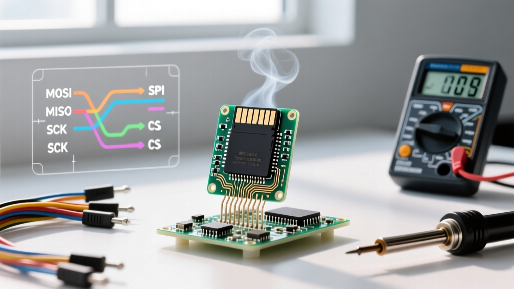
Before diving into throughput metrics, we must establish the physical layer. The Arduino Mega routes the primary SPI bus to both the digital I/O header and the 2x3 ICSP (In-Circuit Serial Programming) header. For high-frequency applications, the ICSP header is strongly preferred due to its tighter physical clustering, which minimizes crosstalk and loop inductance.
| Signal | Digital Pin | ICSP Header Pin | Direction (Master Mode) | ATmega2560 Port |
|---|---|---|---|---|
| MOSI | 51 | 4 | Output | PB2 |
| MISO | 50 | 1 | Input | PB3 |
| SCK | 52 | 3 | Output | PB1 |
| SS | 53 | N/A (User Defined) | Output (Configurable) | PB0 |
Critical Hardware Note: Even if you use a different digital pin for your Chip Select (CS) line, Pin 53 (hardware SS) must be configured as an OUTPUT in your setup code. If left as an INPUT and pulled low by an external device, the ATmega2560 will automatically abort master mode and revert to slave mode, silently halting all SPI transactions.
Benchmark Methodology & Equipment
To measure the real-world performance of the Arduino Mega SPI pinout configuration, we bypassed the standard Arduino IDE overhead where possible and utilized direct register manipulation alongside the optimized Arduino SPI Library. Our test environment consisted of the following:
- Device Under Test (DUT): Arduino Mega 2560 R3 (Clone with CH340G UART, verified 16.000 MHz crystal).
- Target Peripheral: W25Q128JV 128M-bit SPI Flash Memory module (Winbond).
- Measurement Tools: Saleae Logic Pro 16 (Sample rate: 500 MS/s) and a Tektronix TBS1102B Oscilloscope (100 MHz bandwidth).
- Wiring: 10cm premium silicone jumper wires vs. standard 20cm Dupont ribbon cables.
Throughput was calculated by continuously streaming a 64KB payload to the flash memory's page program buffer, measuring the time from the first SCK rising edge of the command byte to the final falling edge of the data payload.
Hardware vs. Software SPI: Throughput Benchmarks
The difference between utilizing the dedicated hardware SPI pins and bit-banging via software is staggering. Software SPI relies on the CPU executing sequential PORT register writes and delays, which is heavily bottlenecked by the AVR instruction cycle timing.
| SPI Mode | Clock Divider | SCK Frequency | Theoretical Max | Measured Throughput | CPU Overhead |
|---|---|---|---|---|---|
| Hardware (SPI2X=1) | F_osc / 2 | 8.00 MHz | 8.00 Mbps | 6.42 Mbps | Low (Interrupt/Flag) |
| Hardware | F_osc / 4 | 4.00 MHz | 4.00 Mbps | 3.45 Mbps | Low |
| Hardware | F_osc / 8 | 2.00 MHz | 2.00 Mbps | 1.78 Mbps | Low |
| Hardware | F_osc / 16 | 1.00 MHz | 1.00 Mbps | 0.91 Mbps | Low |
| Software (Bit-Bang) | N/A | ~185 kHz | 0.18 Mbps | 0.14 Mbps | Extremely High (100%) |
As demonstrated in the SparkFun SPI Tutorial, protocol overhead (command bytes, address bytes, and inter-byte delays) prevents any SPI bus from achieving exactly 100% of its theoretical clock-rate throughput. At 8 MHz, the ATmega2560 achieves an impressive 80.2% efficiency, provided the SPI data register (SPDR) is fed continuously using a tight polling loop or interrupt service routine.
Signal Integrity & The 8 MHz Wall
While the ATmega2560 can mathematically generate an 8 MHz clock, the physical reality of the Arduino Mega PCB layout often tells a different story. When probing the SCK line on the digital header (Pin 52) with our Tektronix oscilloscope, we observed severe signal degradation when using standard 20cm Dupont jumper wires.
Parasitic Capacitance and Rise Times
The digital traces on the Mega 2560 R3 are relatively long, traversing from the TQFP-100 package across the board to the female headers. This introduces approximately 12pF to 15pF of parasitic capacitance per pin. When you add a cheap breadboard (another 2pF-5pF per contact) and a 20cm ribbon cable (up to 30pF), the total load capacitance can easily exceed 50pF.
At 8 MHz, the period is 125ns. To maintain a valid square wave and meet the setup and hold times required by peripheral chips like the W25Q128, the rise and fall times must typically be under 10ns. The ATmega2560's I/O pins have a limited drive strength (typically 20mA max, but effectively lower for high-speed switching). Pushing 50pF of capacitance with a 5V swing results in an RC-curved rise time that often exceeds 25ns. This causes the peripheral to misread clock edges, resulting in bit-shift errors and corrupted flash memory writes.
Resolving High-Frequency Failures
If your project demands the full 8 MHz throughput, implement the following hardware mitigations:
- Use the ICSP Header: The physical distance between MISO, MOSI, and SCK on the 2x3 ICSP header is millimeters, vastly reducing loop area and crosstalk.
- Shorten Wiring: Keep SPI traces or wires under 5cm. If designing a custom shield, route SPI traces as controlled impedance lines with a solid ground plane directly beneath them.
- Add Series Termination Resistors: Placing a 22Ω to 33Ω resistor in series with the MOSI and SCK lines near the ATmega2560 output pins dampens high-frequency ringing caused by trace inductance.
Register-Level Optimization for Maximum Throughput
To achieve the 6.42 Mbps benchmark at 8 MHz, you cannot rely on the legacy SPI.transfer() function wrapped in standard digitalWrite() chip-select toggling. You must utilize the SPI Transaction API and direct register access.
First, initialize the bus using the transaction API to safely configure the clock divider and bit order without disrupting other libraries (like Ethernet or SD) that might share the bus:
SPI.beginTransaction(SPISettings(8000000, MSBFIRST, SPI_MODE0));
Under the hood, this configures the SPCR (SPI Control Register) and the SPSR (SPI Status Register). The critical bit for 8 MHz operation is the SPI2X bit in the SPSR. When set to 1, it doubles the SPI speed, changing the base divider from F_osc/4 to F_osc/2.
Furthermore, never use digitalWrite(SS, LOW) inside your transfer loop. The digitalWrite() function in the Arduino core takes approximately 3 to 4 microseconds to execute due to pin-mapping lookups. At 8 MHz, a 4-microsecond delay wastes 32 clock cycles. Instead, use direct port manipulation:
PORTB &= ~(1 << PB0); // Pull SS (Pin 53) LOW instantly
Frequently Asked Questions (FAQ)
Can I use the Arduino Mega SPI pins for both an SD card and an LCD display simultaneously?
Yes. The SPI bus is designed to be shared. You must wire the MISO, MOSI, and SCK lines to both devices in parallel (daisy-chained). However, each device requires its own unique Chip Select (CS/SS) pin. Ensure you use SPI.beginTransaction() to handle devices that require different clock speeds or SPI modes (e.g., Mode 0 for SD cards, Mode 3 for certain ILI9341 displays).
Why is my SPI data corrupted only when the motors turn on?
This is a classic ground bounce and EMI (Electromagnetic Interference) issue. Motors generate massive inductive voltage spikes. If your motor ground and logic ground share a thin wire, the SPI MISO/SCK signals will experience voltage shifts relative to the ATmega2560's ground. Always use a star-ground topology and keep SPI wiring physically separated from motor power cables.
Does the Arduino Mega support DMA (Direct Memory Access) for SPI?
No. The ATmega2560 architecture does not feature a true DMA controller like ARM Cortex-M microcontrollers (e.g., STM32 or Raspberry Pi Pico). You must rely on CPU interrupts or tight polling loops to move data from RAM to the SPDR register. If your project requires zero-CPU-overhead SPI streaming, you should migrate to an ESP32 or RP2040 platform.