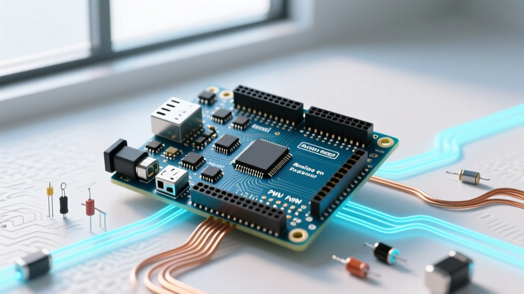

Evaluating the Arduino Mega Pin Architecture for Complex Builds
When designing embedded systems that require extensive sensor arrays, multiple motor drivers, or complex communication buses, the standard 14-pin Arduino Uno quickly becomes a bottleneck. Enter the Arduino Mega 2560. Built around the Microchip ATmega2560 microcontroller, this board is the undisputed heavyweight in the legacy 8-bit AVR lineup. However, simply having more pins does not automatically make it the right choice for every high-I/O project. Understanding the specific capabilities, hardware constraints, and memory mapping of every arduino mega pin is critical for engineers and advanced makers in 2026.
While genuine Arduino Mega 2560 Rev3 boards retail for approximately $48 to $52 USD, high-quality third-party clones utilizing the CH340G USB-to-serial chip can be sourced for $14 to $18 USD. Regardless of the manufacturer, the underlying ATmega2560 silicon dictates strict electrical and logical boundaries. According to the official Arduino Mega 2560 documentation, the board features 54 digital input/output pins and 16 analog inputs. But how do these pins actually perform under the stress of real-world industrial or advanced hobbyist applications?
Digital I/O and Timer Associations
The Mega offers 54 digital I/O pins (D0 to D53), operating at a strict 5V logic level. Of these, 15 pins support hardware Pulse Width Modulation (PWM): pins 2 through 13, and pins 44, 45, and 46. However, not all PWM pins are created equal. The ATmega2560 utilizes six hardware timers (Timer0, Timer1, Timer3, Timer4, and Timer5, plus Timer2).
Timer Conflicts and PWM Resolution
- Timer0 (8-bit): Controls pins 4 and 13. Crucially, Timer0 is hardwired to the
millis()anddelay()functions in the Arduino core. Altering its prescaler to change PWM frequency will break system timing. - Timer1, 3, 4, 5 (16-bit): Control the majority of the remaining PWM pins. These 16-bit timers allow for high-resolution PWM generation, which is essential for precision servo control and LED dimming without visible flicker.
- Timer2 (8-bit): Controls pins 9 and 10. Often used by the
Tonelibrary, which will render these pins unusable for standard PWM if audio generation is active.
If your project requires more than 15 PWM channels, you must pivot to software-based PWM (like the analogWrite emulation libraries) or external hardware like the PCA9685 16-channel I2C PWM driver.
Analog Inputs and ADC Limitations
The board provides 16 analog input channels (A0 to A15), doubling the capacity of the Uno. These pins feed into a single internal 10-bit Successive Approximation Register (SAR) Analog-to-Digital Converter (ADC). This means analog readings map to integer values between 0 and 1023, representing 0V to the reference voltage (default 5V, yielding a resolution of ~4.88mV per step).
Expert Insight: If your project demands higher precision (e.g., load cells or high-fidelity audio sampling), the Mega's internal 10-bit ADC is insufficient. For 16-bit or 24-bit resolution, bypass the internal ADC entirely and utilize the SPI header (pins 50-53) to interface with an external ADC like the ADS1115 or ADS1256.
Communication Bus Pin Mapping
One of the most compelling reasons to choose the Mega is its robust hardware communication support. Unlike smaller boards that rely on software-emulated serial ports, the Mega features dedicated hardware peripherals.
- UART (Serial): Four hardware serial ports.
Serial(Pins 0, 1) is shared with the USB interface.Serial1(Pins 19, 18),Serial2(Pins 17, 16), andSerial3(Pins 15, 14) are fully independent, allowing simultaneous communication with GPS modules, cellular modems, and RS-485 transceivers without blocking the main processor. - I2C (TWI): Located on pins 20 (SDA) and 21 (SCL). Note that unlike the Uno R3, the Mega does not route I2C exclusively to the dedicated header near the USB port; it is strictly bound to D20 and D21 on the main digital header.
- SPI: Located on pins 50 (MISO), 51 (MOSI), 52 (SCK), and 53 (SS). The SPI header is also broken out on the 6-pin ICSP cluster, ensuring compatibility with shields that rely on the ICSP footprint rather than the digital pins.
Project Suitability Matrix
To determine if the Arduino Mega pin layout aligns with your project requirements, consult the suitability matrix below.
| Project Type | Pin Requirement Profile | Mega Suitability | Recommended Alternative |
|---|---|---|---|
| Multi-Axis CNC Router | High PWM, Step/Dir outputs, Limit switches | Excellent (Ample digital I/O and 16-bit timers) | None (Mega is standard for GRBL) |
| Home Automation Hub | Multiple UARTs, Ethernet, I2C sensors | Good (4x Hardware UARTs) | ESP32-S3 (Better for WiFi/MQTT) |
| High-Speed Data Logging | Fast ADC sampling, SD card SPI | Poor (10-bit ADC, 16MHz clock limits throughput) | Teensy 4.1 (32-bit, 600MHz) |
| Robotic Arm Controller | 10+ Servos, I2C displays, Serial telemetry | Excellent (Native Servo library support) | Arduino Portenta H7 (If vision is needed) |
Hardware Constraints and Edge Cases
When designing custom PCB shields or wiring harnesses for the Mega, you must respect the electrical limits of the ATmega2560 silicon. The Microchip ATmega2560 datasheet specifies an absolute maximum DC current per I/O pin of 40mA. However, operating continuously at 40mA will degrade the silicon over time and cause voltage sag. A safe continuous design limit is 20mA per pin.
Furthermore, the combined current draw across all VCC and GND pins must not exceed 200mA. If you attempt to power multiple relays or high-brightness LEDs directly from the digital pins, you will trigger the board's polyfuse or, worse, permanently damage the microcontroller's internal I/O buffers. Always use logic-level MOSFETs (like the IRLZ44N) or optocouplers to isolate high-current loads from the Mega's delicate 5V logic pins.
The Pin 53 (SS) Gotcha
Pin 53 serves as the hardware Slave Select (SS) pin for the SPI bus. Even if your project uses a different pin to control the chip select of an SPI device (like an SD card module), Pin 53 must be configured as an OUTPUT or kept HIGH. If Pin 53 is left as an INPUT and is pulled LOW by stray noise, the ATmega2560 will automatically revert to SPI Slave mode, causing the master SPI bus to crash silently. This is a notorious edge case that traps many developers transitioning from the Uno to the Mega.
Advanced Optimization: Direct Port Manipulation
Using the standard digitalWrite() function on the Mega incurs significant overhead. The Arduino core must translate the pin number to the corresponding AVR port and bit, which takes roughly 4 to 5 microseconds. In high-speed applications, such as multiplexing LED matrices or reading high-frequency encoders, this latency is unacceptable.
By utilizing direct port manipulation, you can toggle multiple arduino mega pin states simultaneously in a single clock cycle (62.5 nanoseconds). For example, writing directly to PORTA controls pins 22 through 29 simultaneously. The Arduino Bit Math and Port Manipulation Guide details how to use registers like DDRA (Data Direction Register) and PORTA (Output Register) to bypass the Arduino abstraction layer entirely. This technique is mandatory for projects requiring sub-microsecond timing precision on the Mega's digital headers.
Final Verdict on Platform Selection
The Arduino Mega 2560 remains a highly relevant platform in 2026 for projects demanding massive amounts of 5V-tolerant digital I/O and multiple hardware serial ports. Its physical footprint and pin layout have made it the standard for 3D printer control boards (like the RAMPS 1.4) and CNC shields. However, for projects requiring high-speed processing, native wireless connectivity, or high-resolution analog sampling, engineers should look toward modern 32-bit alternatives like the Teensy 4.1 or the ESP32-S3, reserving the Mega strictly for high-pin-count, low-to-medium frequency I/O tasks.