
Introduction to TAEC Component Safety and Reliability
As power electronics and embedded systems continue to demand higher efficiency and smaller form factors in 2026, the components we integrate must be handled with absolute precision. Toshiba America Electronic Components Inc (TAEC) supplies a vast portfolio of discrete semiconductors, system LSI, and optoelectronics that form the backbone of modern motor drives, automotive inverters, and industrial power supplies. However, the inherent sensitivity of these advanced silicon and wide-bandgap devices means that improper handling, assembly, or thermal management can lead to catastrophic field failures.
This guide outlines the critical safety protocols and best practices for integrating Toshiba MOSFETs and Toshiba Optocouplers into your designs. By adhering to strict Electrostatic Discharge (ESD) mitigation, precise mechanical torque specifications, and Moisture Sensitivity Level (MSL) baking protocols, engineers and technicians can eliminate latent defects and ensure long-term operational reliability.
ESD Mitigation for High-Speed Logic and Power MOSFETs
Electrostatic Discharge remains one of the most pervasive silent killers in semiconductor manufacturing and DIY assembly. While power devices like the TK-series UMOS MOSFETs are rugged in operation, their gate oxides are highly susceptible to ESD damage during handling. According to the ESD Association, human body model (HBM) discharges can easily exceed 10kV in low-humidity environments, far surpassing the typical 2kV HBM rating of most discrete power transistors.
Specific Thresholds for TK-Series Devices
Take the TK80E10N1 (100V, 80A N-channel MOSFET) as a prime example. Its internal gate structure is optimized for low switching losses, which inherently thins the gate oxide layer. This results in a typical HBM rating of 2kV and a Charged Device Model (CDM) rating of 1kV. A CDM event is particularly dangerous during automated pick-and-place operations, as the component itself becomes charged and discharges rapidly upon contact with the solder pad.
- Wrist Straps and Footwear: All personnel handling TAEC bare components must wear continuous monitors connected to a common point ground, maintaining a resistance between 750kΩ and 35MΩ.
- Ionization: For automated SMT lines processing Toshiba surface-mount logic (e.g., TC7S series), inline ionizers must be calibrated to neutralize charges within 2 seconds at a distance of 30cm.
- Faraday Cages: Never transport TAEC components outside of their metallized static-shielding bags. Once opened, the components must remain within an EPA (ESD Protected Area) until reflow soldering is complete.
Thermal Management and Mechanical Mounting Torque
Thermal runaway is a primary failure mode in high-current applications. Toshiba America Electronic Components Inc designs their power discretes with specific thermal resistance profiles that assume perfect mechanical mating between the device package and the heatsink. Over-tightening mounting screws can crack the silicon die or delaminate the package epoxy, while under-tightening leaves microscopic air gaps that drastically increase junction-to-ambient thermal resistance ($\theta_{JA}$).
Package Specifications and Torque Limits
When mounting through-hole power devices, always use a calibrated torque screwdriver. The following table outlines the precise mechanical and thermal specifications for common TAEC power packages used in 2026 inverter designs.
| Package Type | Typical TAEC Device | $\theta_{JC}$ (°C/W) | Mounting Torque (N·m) | Max Junction Temp (°C) |
|---|---|---|---|---|
| TO-220-4L | TK80E10N1 | 0.83 | 0.49 - 0.69 | 150 |
| TO-247-3L | TK2R2A08QM | 0.28 | 0.69 - 0.98 | 175 |
| DIP-8 (SMD) | TLP350 | N/A (Soldered) | N/A | 125 |
Note: Always apply a uniform layer of high-performance thermal interface material (TIM) with a thermal conductivity of at least 3.0 W/m·K before applying torque. Tighten screws in a star pattern if multiple fasteners are used.
Moisture Sensitivity and Baking Protocols
Surface-mount components from Toshiba, particularly complex system LSI and SMD optocouplers, are highly susceptible to the "popcorn effect" during reflow soldering. Moisture absorbed into the plastic encapsulation rapidly turns to steam when exposed to 260°C reflow temperatures, causing internal delamination or package cracking.
IPC/JEDEC J-STD-020 Compliance: Components rated MSL 3 or higher must be baked if their factory-sealed moisture barrier bag (MBB) has been open beyond the specified floor life. For MSL 3 (168 hours floor life at ≤30°C/60% RH), exceeding the time limit mandates a 125°C bake for 24 hours prior to assembly.
For high-reliability automotive or aerospace projects utilizing TAEC components, it is a best practice to bake all SMD tape-and-reel inventory for 4 hours at 125°C immediately before loading them into the pick-and-place feeder, regardless of the humidity indicator card (HIC) status. This eliminates any marginal moisture absorption that could compromise long-term reliability.
Soldering Profiles and Optocoupler Edge Cases
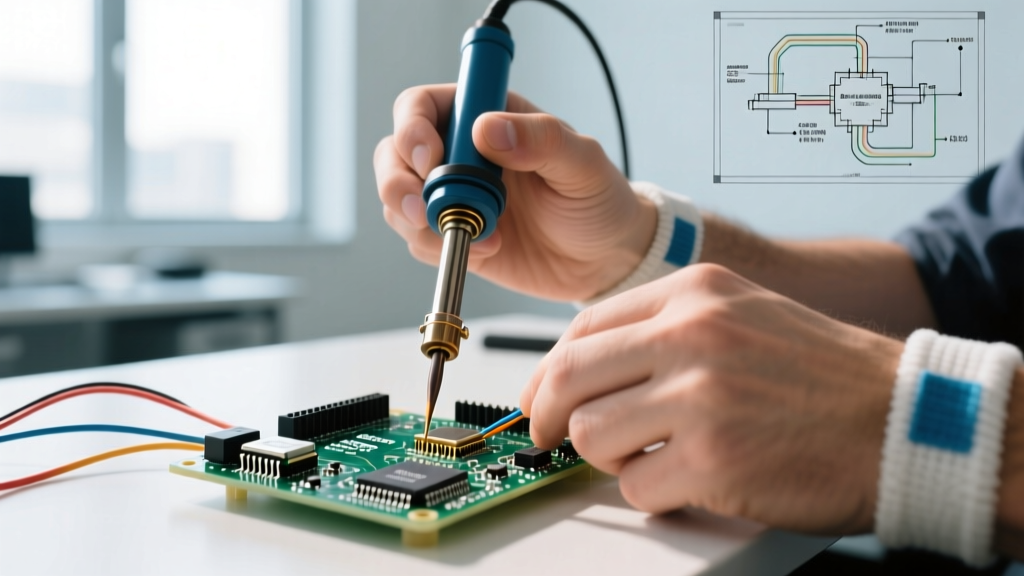
The TLP350 is a staple gate-drive optocoupler used to drive IGBTs and SiC MOSFETs. While robust in operation, its internal LED and CMOS output stage are sensitive to excessive thermal stress during wave or selective soldering. The absolute maximum soldering temperature for the TLP series is 260°C for no more than 10 seconds. Prolonged exposure degrades the LED's luminous efficiency, leading to a gradual drop in the Current Transfer Ratio (CTR) and eventual failure to trigger the gate.
Preventing dV/dt Latch-up in TLP Devices
A frequent field failure mode observed in high-voltage motor drives is not due to thermal or ESD damage, but rather improper bypass capacitor placement. The TLP350 features an internal logic circuit that can latch up if subjected to high common-mode transient immunity (CMTI) noise exceeding 35kV/µs. To prevent this:
- Place a 0.1µF X7R ceramic bypass capacitor within 2mm of the VCC (Pin 8) and GND (Pin 5) pins.
- Ensure the PCB ground plane beneath the optocoupler is solid and unbroken to minimize parasitic inductance.
- Use a dedicated, isolated DC-DC converter with low coupling capacitance (under 10pF) to power the secondary side of the TLP350.
Summary of Best Practices for 2026 Designs
Integrating components from Toshiba America Electronic Components Inc requires a disciplined approach to manufacturing and assembly. By strictly enforcing ANSI/ESD S20.20 protocols, utilizing calibrated torque tools for TO-220 and TO-247 packages, and adhering to rigorous MSL baking schedules, engineering teams can drastically reduce infant mortality rates in their power electronics. Always consult the specific TAEC datasheet for the exact thermal and electrical limits of your chosen device, as continuous improvements in silicon fabrication mean that specifications are frequently updated to push the boundaries of power density and efficiency.