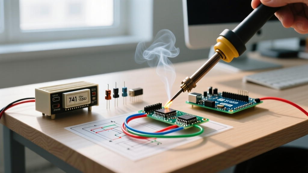

The Hidden Curriculum of Obsolescence
In the 2026 electronics landscape, the lifecycle of a semiconductor often barely outlasts the design cycle of the product it inhabits. Diminishing Manufacturing Sources and Material Shortages (DMSMS) is a critical challenge tracked heavily by organizations like the Defense Logistics Agency. However, for the DIY electronics enthusiast, repair technician, or junior engineer, obsolete electronic components represent a unique, high-value skill-building path.
Working with discontinued parts forces you to move beyond simple "plug-and-play" breadboarding. It demands a deep understanding of semiconductor physics, logic family interoperability, and physical footprint constraints. By learning to resurrect, replace, and reverse-engineer legacy hardware, you build a foundational expertise that makes you a vastly superior circuit designer.
Industry Insight: According to NASA's Electronic Parts and Packaging (NEPP) Program, managing obsolescence in long-lifecycle missions requires rigorous characterization of replacement parts to ensure they meet the exact environmental and electrical margins of the original obsolete components.
Phase 1: Datasheet Archaeology and Parameter Mapping
The first skill you develop when dealing with obsolete electronic components is "datasheet archaeology." When a legacy part like the ubiquitous LM741 operational amplifier becomes hard to source in specific military-spec or through-hole DIP packages, you cannot simply drop in any modern op-amp without consequences.
Failure Mode Analysis: The Op-Amp Swap
Let us examine a common scenario: replacing an aging LM741 in a precision analog sensor circuit. A beginner might swap it for a modern rail-to-rail CMOS op-amp like the OPA192. While the OPA192 is objectively "better" on paper, this swap can break the circuit due to parameter mismatches:
- Input Bias Current: The LM741 uses bipolar junction transistors (BJTs) at the input, resulting in an input bias current of roughly 80nA. The OPA192 uses CMOS, dropping this to 2pA. If the legacy circuit relied on that 80nA bias current flowing through a specific feedback resistor network to establish a DC offset, the CMOS swap will shift the operating point, causing the output to rail.
- Slew Rate and Stability: The LM741 has a notoriously slow slew rate of 0.5V/µs. The OPA192 boasts 20V/µs. In circuits with poor bypassing or parasitic capacitance on the feedback node, the faster modern part will instantly oscillate due to a degraded phase margin.
Skill Acquired: You learn to map not just the "headline" specs, but the secondary parasitic characteristics that define a circuit's actual behavior.
Phase 2: Navigating Logic Family Interoperability
When repairing vintage synthesizers, industrial control relays, or retro-computing hardware, you will frequently encounter the 7400-series logic chips. The 7400-series integrated circuits span multiple incompatible sub-families. Finding a new-old-stock (NOS) 74LS00 (Low-power Schottky) quad NAND gate might be impossible, forcing you to use a 74HC00 (High-speed CMOS).
The Voltage Threshold Trap
Replacing 74LS (Bipolar) with 74HC (CMOS) at a 5V supply is a classic trap that teaches you about logic voltage thresholds:
| Logic Family | Supply Voltage (Vcc) | Min. High-Level Input (V_IH) | Max. Low-Level Input (V_IL) | Output Drive Type |
|---|---|---|---|---|
| 74LS00 (Legacy) | 5.0V | 2.0V | 0.8V | Totem-Pole (Asymmetric) |
| 74HC00 (Modern) | 5.0V | 3.15V | 1.35V | Push-Pull (Symmetric) |
| 74HCT00 (Bridge) | 5.0V | 2.0V | 0.8V | Push-Pull (Symmetric) |
If a legacy 5V microcontroller outputs a logic HIGH of 2.8V, it will successfully drive a 74LS00 (requires 2.0V). However, it will fail to drive a 74HC00 (requires 3.15V), leaving the input in an undefined, high-current-draw linear region. The skill-building solution? You learn to specify the 74HCT family, which marries CMOS power efficiency with TTL-compatible input thresholds.
Phase 3: Physical Footprint Adaptation and PCB Design
Obsolete electronic components are often tied to obsolete physical footprints. The Dual In-line Package (DIP) with a 2.54mm (0.1-inch) pitch is rapidly vanishing from modern semiconductor foundries, replaced by SOIC, QFN, and BGA surface-mount packages.
Designing Drop-In Adapter Boards
When you must replace a discontinued DIP-8 microcontroller or op-amp on an existing through-hole PCB, you must design a custom adapter. This builds critical PCB layout skills:
- Pitch Translation: You must route traces from a 1.27mm (0.05-inch) SOIC-8 pitch to a 2.54mm DIP-8 pitch. This requires mastering trace width and clearance calculations (e.g., using 6-mil traces with 6-mil clearance to escape the SOIC pads).
- Z-Height Constraints: An SOIC-to-DIP adapter adds vertical Z-height. If the legacy enclosure has a tight clearance, you must design the adapter PCB using a 0.4mm thin core FR4 material rather than the standard 1.6mm.
- Cost Optimization: In 2026, prototyping a 5x5cm 2-layer adapter board via services like JLCPCB or PCBWay costs roughly $2 to $5 for a batch of five. Learning to panelize these tiny adapters into a single 10x10cm manufacturing file maximizes yield and minimizes shipping costs.
Phase 4: Scavenging and Component Characterization
The final phase of the skill-building path involves harvesting obsolete components from donor boards and verifying their health. Desoldering a 40-pin DIP FPGA or a rare vintage audio DAC without destroying the part or lifting the PCB pad requires immense thermal discipline.
Tooling and Technique
- Thermal Extraction: Use a dedicated desoldering gun like the Hakko FR-301 (approx. $250) or apply low-temperature bismuth-based solder (e.g., Chip Quik, melting at 58°C) to the joints. This lowers the overall melting point of the joint, allowing extraction at lower iron temperatures (around 200°C) and preventing thermal delamination of the legacy PCB.
- Parasitic Verification: Once removed, the component must be tested. While a multimeter checks for dead shorts, an LCR meter like the DER EE DE-5000 (approx. $95) is essential for characterizing the input capacitance and package inductance of salvaged RF or high-speed digital components to ensure they still meet the original datasheet tolerances.
Conclusion: From Scarcity to Mastery
Dealing with obsolete electronic components is not merely a frustrating exercise in supply chain management; it is a rigorous, hands-on masterclass in electrical engineering. By forcing you to understand why a component behaves the way it does, rather than just accepting its black-box functionality, obsolescence transforms you from a simple parts assembler into a true circuit architect. The next time you face a discontinued part, view it as an invitation to level up your diagnostic, design, and adaptation skills.


