
Transitioning to Micro-Scale Electronics
For hobbyists and junior technicians, moving from through-hole technology (THT) to surface-mount devices (SMD) represents a massive leap in capability. Modern precision electronic components—ranging from microscopic 0402 resistors to dense 64-pin QFP microcontrollers—demand a fundamental shift in how you approach thermal management, tooling, and physical handling. Unlike THT components that rely on mechanical friction before soldering, SMD parts are held in place entirely by the surface tension of molten solder and the tackiness of chemical flux.
This tutorial bridges the gap between basic soldering and professional micro-electronics assembly. We will cover the exact tooling required in 2026, the physics of drag soldering, and the strict environmental protocols necessary to prevent catastrophic component failure.
Pro-Tip: The Flux is the Real Tool
When working with precision electronic components, your soldering iron merely provides the heat; the flux does the actual work of removing oxidation and guiding the solder via capillary action. Never attempt micro-soldering without a high-quality, no-clean or RMA (Rosin Mildly Activated) flux pen or syringe.
Essential Toolkit for Precision Work
You cannot reliably solder a 0.5mm pitch IC with a standard 60W hardware store iron. Precision electronic components require tools that offer rapid thermal recovery and fine geometric control.
1. Temperature-Controlled Soldering Stations
As of 2026, the Weller WE1010NA (approx. $115) and the Hakko FX-951 (approx. $280) remain the industry benchmarks for bench work. You need a station that can maintain a stable tip temperature within ±5°C. When a large ground plane draws heat away from your iron, a high-wattage, digitally controlled station will inject power instantly to prevent cold joints.
- Tip Selection: Use a micro-pencil (0.4mm) for 0603 passives and a mini-hoof (1.5mm) for drag-soldering SOIC or TSSOP ICs.
- Solder Wire: Ditch standard 0.8mm wire. Purchase Kester 24-6337-8822 or equivalent in 0.3mm (0.015") diameter. For lead-free compliance, use SAC305 (Sn96.5/Ag3.0/Cu0.5); for hobbyist ease, use 63/37 SnPb eutectic.
2. Magnification and ESD-Safe Handling
The human eye cannot reliably inspect a 0.4mm pitch pin for micro-bridges. A trinocular stereo zoom microscope, such as the AmScope SE400-Z ($140-$180), provides the necessary 10x-20x magnification with a 4-inch working distance. Pair this with a diffused LED ring light to eliminate harsh shadows.
Furthermore, precision electronic components are highly susceptible to Electrostatic Discharge (ESD). According to the ESD Association fundamentals, a human walking across a carpet can generate up to 35,000 volts, while modern IC gates can be destroyed by as little as 10 volts. Always use ESD-safe tweezers (e.g., Hakko CHP ESD series, $12) and work on a grounded dissipative mat.
Understanding Metric SMD Sizes
Precision electronic components use standardized metric imperial codes. Understanding these dimensions is critical before you even pick up your tweezers.
| Package Code | Metric Size (L x W) | Imperial Equivalent | Handling Difficulty | Typical Use Case |
|---|---|---|---|---|
| 0201 | 0.6mm x 0.3mm | 008004 | Extreme (Requires Microscope) | High-density smartphones, wearables |
| 0402 | 1.0mm x 0.5mm | 01005 | High (Fine Tweezers Needed) | Modern IoT boards, dense motherboards |
| 0603 | 1.6mm x 0.8mm | 0201 | Moderate (Standard SMD) | General consumer electronics, Arduino shields |
| 0805 | 2.0mm x 1.25mm | 0302 | Easy (Beginner Friendly) | Power rails, LED current limiting |
Step-by-Step: Drag Soldering an SOIC-8 IC
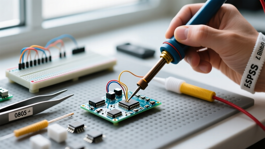
Drag soldering is the most efficient method for attaching multi-pin precision electronic components like SOIC, TSSOP, and QFP chips. Instead of soldering each pin individually, you utilize the surface tension of molten solder and flux to pull the solder evenly across all pins.
- Prep the Pads: Clean the PCB pads with 99% isopropyl alcohol (IPA). Apply a microscopic amount of tacky flux (e.g., Chip Quik SMD291AX) to the pads.
- Tack One Corner: Apply a tiny dab of solder to one corner pad. Using your tweezers, align the IC. Melt the dab to tack the chip in place. Verify alignment on all sides under the microscope.
- Flux the Pins: Generously apply liquid or gel flux across the entire row of pins. Do not skip this step.
- The Drag: Load your mini-hoof tip with a small bead of 0.3mm solder. Set your iron to 320°C (for SnPb) or 350°C (for SAC305). Place the flat of the hoof against the pins at a 45-degree angle. Slowly drag the iron across the pins in one smooth, continuous motion (approx. 1 second per row).
- Wick the Excess: If solder bridges form between pins, apply more flux and use a high-quality copper desoldering braid (e.g., Chemtronics 80-1-5) to wick away the excess. The flux will break the surface tension and pull the bridge into the braid.
Troubleshooting Common Failure Modes
When assembling precision electronic components, physical defects can lead to latent failures that pass initial visual inspection but fail in the field. Adhering to IPC standards for acceptability (IPC-A-610) helps identify these flaws.
Tombstoning (Drawbridging)
The Symptom: A two-terminal passive component stands up on one end, resembling a tombstone.
The Root Cause: Uneven heating of the two pads. If one pad reaches reflow temperature before the other, the surface tension of the molten solder on the first pad pulls the component upright.
The Fix: Ensure your iron tip contacts both the component terminal and the PCB pad simultaneously. Design PCB footprints with symmetrical thermal relief to prevent one pad from sinking heat into a ground plane faster than the other.
Solder Wicking
The Symptom: Solder climbs up the IC lead away from the PCB pad, leaving a starved, weak joint at the base.
The Root Cause: The iron was applied to the top of the IC pin rather than the pad, or excessive flux was placed on the component body.
The Fix: Always heat the PCB pad first. The solder should flow toward the heat source and the flux, not away from the joint interface.
Moisture Sensitivity and Thermal Shock
Beyond soldering technique, environmental handling is critical. Many precision electronic components, particularly ICs with plastic encapsulation, are hygroscopic—they absorb moisture from the ambient air.
According to the IPC/JEDEC J-STD-033 standard, components are assigned a Moisture Sensitivity Level (MSL). If an MSL-3 or MSL-4 component is exposed to room air beyond its designated floor life (often 168 hours), the trapped moisture will rapidly expand into steam when exposed to 245°C reflow temperatures. This causes internal delamination or the "popcorn effect," where the plastic package physically cracks, destroying the silicon die.
Prevention Protocol: If you suspect your precision electronic components have exceeded their floor life, you must bake them before soldering. The NASA Electronic Parts and Packaging (NEPP) program and JEDEC recommend baking components at 125°C for 24 hours in a specialized laboratory oven to drive out absorbed moisture. Never use a standard kitchen oven, as temperature fluctuations and food-grade contaminants will ruin the components.
Frequently Asked Questions
Can I use lead-free solder for precision SMD work?
Yes, but it requires higher temperatures (typically 345°C - 360°C tip temp) and a more aggressive flux chemistry to overcome the poor wetting characteristics of SAC305 alloys. For beginners learning to handle precision electronic components, 63/37 SnPb eutectic solder is highly recommended due to its lower melting point (183°C) and superior surface tension.
How do I clean no-clean flux residue?
Despite the name, "no-clean" flux can leave a sticky, slightly conductive residue that may cause parasitic capacitance in high-frequency RF circuits. Clean it using 99% IPA and a stiff-bristled ESD-safe brush, followed by a blast of compressed air to push the dissolved flux out from under the component bodies.
What is the best way to store unused SMD components?
Keep precision electronic components in their original sealed moisture barrier bags (MBB) with the included desiccant and humidity indicator card. Once opened, store them in a dry cabinet maintained at <10% relative humidity, or use a vacuum sealer to repackage them with fresh silica gel.