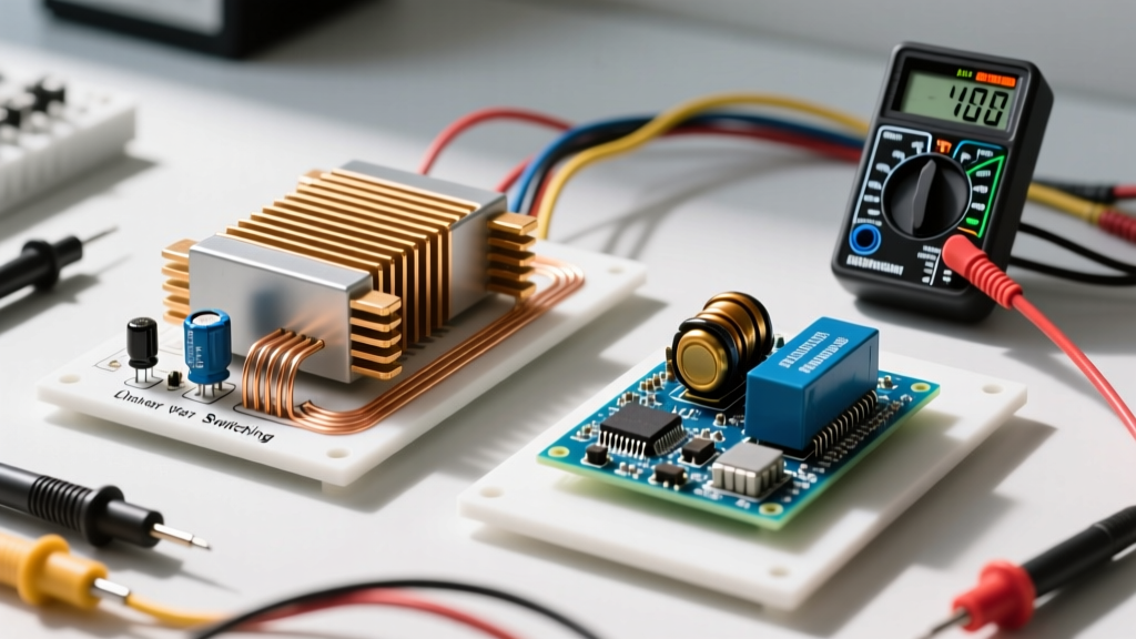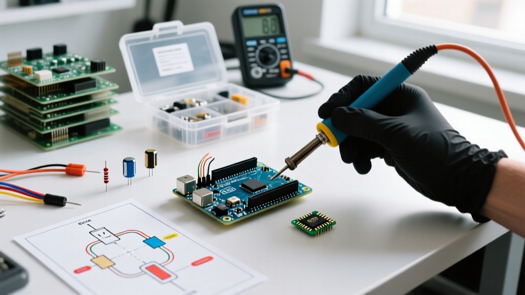

Transitioning from a casual hobbyist to a proficient electronics maker requires more than just following step-by-step tutorials. The true inflection point in your skill-building journey happens when you learn to fluently translate abstract electronic components and symbols on a schematic into physical, three-dimensional parts on a printed circuit board (PCB) or breadboard. In 2026, with the proliferation of dense surface-mount device (SMD) assemblies and complex mixed-signal ICs, this foundational literacy is non-negotiable.
This guide is structured as a progressive skill-building path. We will move from passive foundations to active semiconductors, and finally to electromechanical interfaces, pairing every schematic symbol with its real-world physical counterpart, specific industry part numbers, and common failure modes.
Phase 1: The Passive Foundations
Passive components do not amplify signals or inject power into a circuit, but they dictate the timing, filtering, and current-limiting behavior of every electronic device. The first step in your skill path is recognizing that a single schematic symbol can represent vastly different physical components depending on the application.
| Component | IEEE / IEC Symbol | Common Physical Package | Real-World Failure Mode |
|---|---|---|---|
| Resistor | Zig-zag line (IEEE) or Empty rectangle (IEC) | Through-hole (Vishay MRS25) or SMD (0603) | Thermal drift; SMD pads lifting due to excessive rework heat. |
| Capacitor | Two parallel lines (one curved for polarized) | MLCC (Murata GRM series) or Radial Electrolytic (Nichicon) | MLCC flexure cracking; Electrolytic dielectric drying (high ESR). |
| Inductor | Series of looping arcs or filled rectangles | Shielded SMD (Wurth WE-PD) or Toroidal through-hole | Core saturation leading to thermal runaway; wire insulation breakdown. |
Deep Dive: Capacitor Dielectrics and Markings
Beginners often assume a 10µF capacitor is just a 10µF capacitor. As you advance, you must learn to read the dielectric codes. A ceramic capacitor marked X7R maintains its capacitance reasonably well across temperature changes, whereas a Y5V capacitor can lose up to 80% of its rated capacitance at voltage limits or temperature extremes. When reading SMD ceramic codes, remember they are in picofarads: a code of 106 means 10 followed by 6 zeros (10,000,000 pF), which equals 10µF.
Phase 2: Active Semiconductors
Active components control electron flow using another electrical signal. This is where schematics start to look intimidating, but the physical reality is often simpler than the drawing.
Expert ESD Warning: When handling active SMD components like MOSFETs or microcontrollers, human body model (HBM) electrostatic discharge can instantly destroy the gate oxide. According to the ESD Association standards, always use a grounded wrist strap and an ESD-safe mat when populating active components outside of automated pick-and-place environments.
Transistors: BJT vs. MOSFET
- Bipolar Junction Transistors (BJT): Represented by a circle with an arrow on the emitter. The arrow points out for NPN (e.g., 2N3904) and in for PNP (e.g., 2N3906). BJTs are current-controlled. They are ideal for low-power signal amplification but inefficient for high-current switching due to base current losses.
- Metal-Oxide-Semiconductor FETs (MOSFET): Represented by a channel line with a gate, drain, and source, often featuring an intrinsic body diode arrow. MOSFETs are voltage-controlled. For DIY 5V microcontroller projects, always specify logic-level MOSFETs (like the IRLZ44N) rather than standard-level ones (like the IRF520), which require 10V+ on the gate to fully turn on and will overheat if driven directly from an Arduino GPIO pin.
Integrated Circuits (ICs)
The schematic symbol for an IC is typically a simple rectangle with numbered pins. The physical mapping requires strict attention to the Pin 1 indicator. On physical ICs, Pin 1 is denoted by a laser-etched dot, a beveled edge, or a silkscreen circle on the PCB. Misaligning an IC by a single pin when transitioning from schematic to breadboard is the most common cause of instant, catastrophic component failure (often resulting in the 'magic smoke' release).
Phase 3: Electromechanical Interfaces
Electromechanical components bridge the gap between low-voltage logic and high-voltage/high-current physical work. Properly reading standardized electronic symbols for these parts is critical for safety and isolation.
Relays and Contactors
A relay symbol displays a coil (inductor symbol) mechanically linked to a switch (SPDT or DPDT). In physical space, a common DIY relay is the Omron G5LE-14-DC5. This is a 5V DC coil, SPDT relay capable of switching 10A at 250VAC.
Skill Checkpoint: When designing the physical circuit, you must include a flyback diode (like a 1N4007) in reverse parallel across the relay coil. The schematic symbol for the coil does not inherently show the inductive kickback it generates when de-energized, which will destroy your driving transistor if unprotected. Adhering to rework and modification standards, such as those outlined in the IPC-7711/7721 guidelines, ensures that adding these protective components post-design is done without damaging the PCB pads.
Bridging the Gap: Schematic to Physical PCB
The ultimate test of your skill path is taking a flat schematic and building it in 3D space. Follow this exact workflow to prevent wiring errors:
- Highlight Power Rails: Before placing a single component, use a red pen (or digital highlighter) to trace all VCC/VDD and GND nets on the schematic. Physically wire your breadboard power rails first.
- Group by Functional Blocks: Schematics are drawn for logical flow, not physical proximity. A decoupling capacitor (0.1µF) might be drawn near the power supply on the schematic, but physically, it must be placed within 2mm of the microcontroller's VCC pin to suppress high-frequency noise.
- Verify Pinouts, Not Just Names: A schematic might label a transistor's pins as B, C, and E. The physical TO-92 package for a 2N3904, when viewed from the bottom with the flat side facing you, is actually Emitter, Base, Collector (left to right). Never assume physical pin order matches schematic drawing order.
- Continuity Testing: Before applying power, use a multimeter in continuity mode to check the resistance between VCC and GND. A reading near 0Ω indicates a short circuit (often a misoriented polarized capacitor or a solder bridge).
Essential 2026 Test Equipment for Identification
You cannot master electronic components without the tools to measure their actual physical properties, as real-world components deviate from their theoretical schematic values.
LCR Meters vs. Standard Multimeters
A standard multimeter (like the highly regarded Brymen BM235, retailing around $110) is excellent for measuring DC voltage, current, and basic resistance. However, it cannot accurately measure capacitance or inductance, nor can it display Equivalent Series Resistance (ESR).
For the skill-building path, invest in a dedicated LCR meter. The DER EE DE-5000 (approximately $95) is an industry favorite for hobbyists and pros alike. It allows you to test SMD MLCC capacitors and verify if an electrolytic capacitor has degraded (indicated by a rising ESR value) without desoldering it from the board, provided you use the correct test frequency (usually 100Hz for electrolytics, 1kHz to 100kHz for ceramics).
Skill Path Checkpoints (FAQ)
Why do some schematics use IEC symbols while others use IEEE?
The IEEE (Institute of Electrical and Electronics Engineers) standard is predominantly used in North America, featuring the classic zig-zag resistor. The IEC (International Electrotechnical Commission) standard is used globally and in most modern CAD software (like KiCad or Altium), utilizing a simple rectangular box for resistors. As a maker, you must be fluent in both, though IEC is rapidly becoming the global default.
How do I identify an unmarked SMD component on a salvaged PCB?
Unmarked SMD components are usually ceramic capacitors or small-signal diodes. Ceramic capacitors in the 0603 or 0402 size are almost never marked by the manufacturer. To identify them, you must carefully desolder the component and measure it with an LCR meter. If it reads in the nanofarad or microfarad range, it is a capacitor. If it shows a voltage drop of ~0.3V to 0.7V in one direction on a multimeter's diode mode, it is a semiconductor diode.
What is the most common mistake beginners make with schematic symbols?
Confusing the symbol for a polarized electrolytic capacitor with a non-polarized ceramic capacitor. Placing an electrolytic capacitor in reverse polarity will cause the internal dielectric to break down, generating gas and leading to a violent physical explosion. Always look for the curved line or the '+' sign on the schematic symbol, and match it to the striped negative indicator on the physical capacitor's shrink-wrap sleeve.